This thread has been locked.

If you have a related question, please click the "Ask a related question" button in the top right corner. The newly created question will be automatically linked to this question.

How to select particular channel for ADC in TIVA C when we used more than one channel

Other Parts Discussed in Thread: TM4C123GH6PM

Hello,

I'm using Tiva C (TM4C123GH6PM)

I want to use 3 channels of ADC0, 

I have successfully done for one channel and in that, I trigger ADC using a timer and also used ADC0SS3_Handler for getting results.

When I want to use 3 channels, I don't understand how to take a reading(data) from a particular channel. 

My application is to measure the 3 phase AC voltage.

Thank you 

  • Hi,

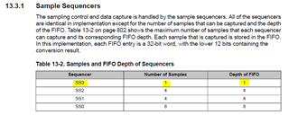
      First of all, you cannot use SS3. SS3 only supports one channel. If you want to take 3 samples, you need to use other sample sequencers such as SS0, SS1 or SS2. See below from the datasheet. 

    Below is an example for configuring three channels using SS0. 

        /* PE3 - AIN0
         * PE2 - AIN1
         * PE1 - AIN2
         */
    
        GPIOPinTypeADC(GPIO_PORTE_BASE, GPIO_PIN_3 | GPIO_PIN_2 | GPIO_PIN_1);
    
        ADCSequenceConfigure(ADC0_BASE, 0, ADC_TRIGGER_PROCESSOR, 0);
    
        ADCSequenceStepConfigure(ADC0_BASE, 0, 0, ADC_CTL_CH0 );
    
        ADCSequenceStepConfigure(ADC0_BASE, 0, 1, ADC_CTL_CH1 );
    
        ADCSequenceStepConfigure(ADC0_BASE, 0, 2, ADC_CTL_CH2 | ADC_CTL_IE |
                                 ADC_CTL_END);
    

  • Dear  Charles,

    Thank you very much for your explanation.

    I Understand well but unfortunately, I used register level programming, Hence I need some more help

    firstly I configure ADC0 and SSO since I want to use 3 channel of ADC0. secondly, I trigger ADC using TIMER, and finally, I take the reading using the interrupt method.

    I understand that the first sample from SS0 is the reading of AN0, 2nd the value of FIFO is the reading of AN1 but I don't understand how to take a reading separately (or how to distinguish) from each channel in ADC0SS0_Handler. since every sample it enable the interrupt.

    So, here is my code, kindly check it and made the necessary changes.

    #include "TM4C123GH6PM.h"
    #include <stdio.h>
    
    SYSCTL->RCGCGPIO |= 0xFF;    /* enable clock to all port *
    SYSCTL->RCGCWTIMER |= 1;     /* enable clock to WTimer Block 0 */
    SYSCTL->RCGCADC |= 1;       /* enable clock to ADC0 */
    
    /* initialize PE3 for AIN0, AIN1, AIN2 input  */
    GPIOE->AFSEL |=7 ;       /* enable alternate function */
    GPIOE->DEN &= ~7;        /* disable digital function */
    GPIOE->AMSEL |= 7;       /* enable analog function */
    	
    	
     ADC0->ACTSS &= ~1;         /* disable SS0 during configuration */   
     ADC0->EMUX |= 0x0005;      /* timer trigger conversion seq 0 */
     ADC0->SSMUX0 = 0x0011;     /* get input from channel 0 ,1,2 */
     ADC0->SSCTL3 |= 0x0644; 000 0110 0100 0100       /* The 3rd sample is the last sample of the sequence and 
                                /*The raw interrupt signal (INR0 bit) is asserted at the end of the 1st, 2nd , 3rd sample's conversion.
     ADC0->IM     |= (1<<0);    /* Unmask ADC0 sequence 0 interrupt*/ 
     ADC0->ACTSS |= 1;         /* enable ADC0 sequencer 0 */
     ADC0->PSSI |= (1<<0);     /* Enable SS0 conversion or start sampling data from AN0,AN1,AN2 */	
     
     /* initialize wtimer 0 to trigger ADC at 1 sample/sec */
     WTIMER0->CTL = 0;            /* disable WTimer before initialization */
     WTIMER0->CFG = 0x04;         /* 32-bit option */
     WTIMER0->TAMR = 0x02;        /* periodic mode and down-counter */
     WTIMER0->TAILR = 160000;       /* WTimer A interval load value reg */
     WTIMER0->CTL |= 0x20;        /* timer triggers ADC */
     WTIMER0->CTL |= 0x01;        /* enable WTimer A after initialization */
    
    NVIC->ISER[0] |= 0x00001110; /* enable IRQ14 for ADC0SS0*/
    
    while(1)
        {	
    	}
    	
    	
    void ADC0SS0_Handler(void){
    
        int value = ADC0->SSFIFO0;     /* dave the sample value*/
    	ADC0->ISC = 1;                 /* clear coversion clear flag bit*/
    	ADC0->PSSI |= (1<<3);          /* Enable SS3 conversion or start sampling data from AN0*/
     
    }
    

    Thank you 

  • HI,

      First of all, please refer to the item 4 in the below FAQ. Basically, we do not support DRM style of coding. If you must use DRM for your project then you can read the source code of these API (e.g. ADCSequenceStepConfigure) on how they are done. 

    https://e2e.ti.com/support/microcontrollers/arm-based-microcontrollers-group/arm-based-microcontrollers/f/arm-based-microcontrollers-forum/695568/faq-faqs-for-tm4c-arm-cortex-m4f-microcontrollers

    Download TivaWare and go to C:\ti\TivaWare_C_Series-2.2.0.295\driverlib2\adc.c. I'm also attaching the file here for your reference. 6305.adc.c5381.adc.h

    I understand that the first sample from SS0 is the reading of AN0, 2nd the value of FIFO is the reading of AN1 but I don't understand how to take a reading separately (or how to distinguish) from each channel in ADC0SS0_Handler. since every sample it enable the interrupt.

    With that said, I can provide some explanation here. If you look at how the API is used to setup the channels, you can see that only channel 2 is enabled for interrupt, not every channel. I think that is an incorrect assumption from your side. In this example, three samples are taken from channel 0, 1 and 2. In the third line of code below, the channel 2 is specified as the last channel in the sequencer 0. This is how sequencer 0 knows that there are only 3 channels in the group. In addition, channel 2 is enabled for interrupt. What this will do is that the sequencer will take 3 samples from channel 0, 1 and 2. Only when channel 2 is sampled will an interrupt generate. Once the interrupt is generated your application will read 3 sample values in the ISR and your application should know that the 3 samples are corresponding to channel 0, 1, and 2. 

    ADCSequenceStepConfigure(ADC0_BASE, 0, 0, ADC_CTL_CH0 );

    ADCSequenceStepConfigure(ADC0_BASE, 0, 1, ADC_CTL_CH1 );

    ADCSequenceStepConfigure(ADC0_BASE, 0, 2, ADC_CTL_CH2 | ADC_CTL_IE |
    ADC_CTL_END);