Part Number: EK-TM4C1294XL
I am using the EK-TM4C1294XL to measure 4 analog channels (CH11, CH10, CH8, CH9). I am using sequence 0 to collect the data using 4 steps. CH11 is collected on step 0, CH10 on step 1, CH8 on step 2, CH9 on step 3. Each ADC pin is connected to 1.65V though a voltage divider of two 10K resistors connected between the launch pad's 3.3V and GND.
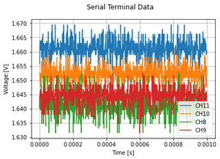
Bellow is a plot of the data that is collected. I am expecting each channel to read ~1.65V but there is a large ~0.2V offset on CH11 collected on step 0.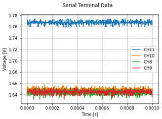
If I switch which channels are collected on the steps , ex collect CH10 on step 0 and CH11 on step 1, the offset follows the sequence step and not the analog channel. I have not been able to figure out why this offset is occurring. Have I missed some setup or configuration?
Here is my code.
#include <stdbool.h>
#include <stdint.h>
#include "inc/hw_ints.h"
#include "inc/hw_memmap.h"
#include "inc/hw_adc.h"
#include "inc/hw_types.h"
#include "inc/hw_udma.h"
#include "driverlib/adc.h"
#include "driverlib/debug.h"
#include "driverlib/gpio.h"
#include "driverlib/interrupt.h"
#include "driverlib/pin_map.h"
#include "driverlib/rom.h"
#include "driverlib/rom_map.h"
#include "driverlib/sysctl.h"
#include "driverlib/systick.h"
#include "driverlib/timer.h"
#include "driverlib/uart.h"
#include "driverlib/udma.h"
#include "utils/uartstdio.h"
#include "driverlib/flash.h"

uint32_t g_ui32SysClock;

//
// Configure the UART and its pins.  This must be called before UARTprintf().
//
void ConfigureUART(void)
{
    //
    // Enable the GPIO Peripheral used by the UART.
    //
    SysCtlPeripheralEnable(SYSCTL_PERIPH_GPIOA);

    //
    // Enable UART0.
    //
    SysCtlPeripheralEnable(SYSCTL_PERIPH_UART0);

    //
    // Configure GPIO Pins for UART mode.
    //
    GPIOPinConfigure(GPIO_PA0_U0RX);
    GPIOPinConfigure(GPIO_PA1_U0TX);
    GPIOPinTypeUART(GPIO_PORTA_BASE, GPIO_PIN_0 | GPIO_PIN_1);

    //
    // Initialize the UART for console I/O.
    //
    UARTStdioConfig(0, 115200, g_ui32SysClock);
}

//
// This function will initialize ADC0 sequence 0 for 4 steps
//
void Init_ADC0_debug()
{
    //
    // Disable the ADC0 sequence 0 interrupt on the processor (NVIC).
    //
    IntDisable(INT_ADC0SS0);

    //
    // Disable interrupts for ADC0 sample sequence 0 to configure it.
    //
    ADCIntDisable(ADC0_BASE, 0);

    //
    // Set the ADC reference
    //
    ADCReferenceSet(ADC0_BASE, ADC_REF_INT);

    //
    // Set the ADC clock speed
    //
    ADCClockConfigSet(ADC0_BASE, ADC_CLOCK_RATE_FULL | ADC_CLOCK_SRC_PIOSC , 1);

    //
    // Disable ADC0 sample sequence 0.  With the sequence disabled, it is now
    // safe to load the new configuration parameters.
    //
    ADCSequenceDisable(ADC0_BASE, 0);

    //
    // Enable sample sequence 0 with a processor signal trigger
    //
    ADCSequenceConfigure(ADC0_BASE, 0, ADC_TRIGGER_PROCESSOR, 0); //ADC_TRIGGER_ALWAYS

    //
    // Configure step 0,1,2,3 on sequence 0, Sample all channels in single-ended mode
    // Set end of sequence and interrupt on the last step
    //
    ADCSequenceStepConfigure(ADC0_BASE, 0, 0, ADC_CTL_CH11 );
    ADCSequenceStepConfigure(ADC0_BASE, 0, 1, ADC_CTL_CH10 );
    ADCSequenceStepConfigure(ADC0_BASE, 0, 2, ADC_CTL_CH8 );
    ADCSequenceStepConfigure(ADC0_BASE, 0, 3, ADC_CTL_CH9 | ADC_CTL_END | ADC_CTL_IE);

    //
    // Since sample sequence 0 is now configured, it must be enabled.
    //
    ADCSequenceEnable(ADC0_BASE, 0);

    //
    // Clear the interrupt status flag.  This is done to make sure the
    // interrupt flag is cleared before we sample.
    //
    ADCIntClear(ADC0_BASE, 0);
}

int main(void)
{

    uint32_t ADC0SS0_FIF0[4];

    //
    // Setup system clock to run from the PLL at 120 MHz.
    //
    g_ui32SysClock = SysCtlClockFreqSet((SYSCTL_XTAL_25MHZ | SYSCTL_OSC_MAIN | SYSCTL_USE_PLL | SYSCTL_CFG_VCO_480), 120000000);

    //
    // Enable the peripherals used by this application.
    //
    SysCtlPeripheralEnable(SYSCTL_PERIPH_ADC0);
    SysCtlPeripheralEnable(SYSCTL_PERIPH_GPIOE);
    SysCtlPeripheralEnable(SYSCTL_PERIPH_GPIOJ);
    SysCtlPeripheralEnable(SYSCTL_PERIPH_GPIOB);

    //
    // Enable I/O
    //
    GPIOPinTypeGPIOInput(GPIO_PORTJ_BASE,GPIO_PIN_0 | GPIO_PIN_1);                                              //Buttons
    GPIOPadConfigSet(GPIO_PORTJ_BASE, GPIO_PIN_0 | GPIO_PIN_1, GPIO_STRENGTH_4MA, GPIO_PIN_TYPE_STD_WPU);       //Pull-ups for buttons

    //
    // Enable ADC pins
    //
    GPIOPinTypeADC(GPIO_PORTB_BASE, GPIO_PIN_4 | GPIO_PIN_5 );                                                  // analog ch10,11
    GPIOPinTypeADC(GPIO_PORTE_BASE, GPIO_PIN_4 | GPIO_PIN_5 );                                                  //Analog ch9,8

    //
    // Initialize UART0 and write initial status.
    //
    ConfigureUART();

    //
    // Initialize the ADC
    //
    Init_ADC0_debug();

    //
    // Enable processor interrupts.
    //
    IntMasterEnable();

    while(1)
    {

        //
        // Start the data collection when button 1 is pressed
        //
        if( GPIOPinRead(GPIO_PORTJ_BASE,GPIO_PIN_0) == 0){


            // Capture a single data point from the ADC
            ADCProcessorTrigger(ADC0_BASE, 0);
            while(!ADCIntStatus(ADC0_BASE, 0, false)) {}                    // Wait for pending ADC conversion to finish
            ADCIntClear(ADC0_BASE, 0);                                      // Stores ADC value automatically to FIFO array
            ADCSequenceDataGet(ADC0_BASE, 0, ADC0SS0_FIF0);

            //
            // Send ADC values over terminal
            //
            uint32_t count;
            for(count = 0; count < 4; count++){

                UARTprintf("%i\n",ADC0SS0_FIF0[count]);
            }


        }


    }

}