Hello,
my name is Philip Schröder, I am currently developing an abstraction in C++ for interrupts with a direct application of but not restricted to GPIOs on an AM64x Sitara board (currently switchign to AM243x, but that should not matter here). I am working with TIs MCU+ SDK here.
In a realted question here:
https://e2e.ti.com/support/microcontrollers/arm-based-microcontrollers-group/arm-based-microcontrollers/f/arm-based-microcontrollers-forum/1063028/am64x-understanding-interrupts/3990053?tisearch=e2e-sitesearch&keymatch=%2520user%253A500371#3990053
Frank Livingston graciously provided me with an example program using various kinds of TISCI IRQ request messages.
One question of mine was here concerning the line:
rmIrqSetReq.src_index = TISCI_BANK_SRC_IDX_BASE_GPIO1 + GPIO_GET_BANK_INDEX(GPIO_PUSH_BUTTON_PIN);
I asked where he got that value for TISCI_BANK_SRC_IDX_BASE_GPIO1 from, where he said it can be deduced from the local base value (lbase) of the interrupt path in (see his comment) drivers/sciclient/soc/am64x_am243x/sciclient_irq_rm.c, line 786
const struct Sciclient_rmIrqIf GPIO1_gpio_bank_90_98_to_MAIN_GPIOMUX_INTROUTER0_in_180_188 = {
    .lbase = 90,
    .len = 9,
    .rid = TISCI_DEV_MAIN_GPIOMUX_INTROUTER0,
    .rbase = 180,
};
While I cannot expect the users of my abstraction to look into some interrupt path definitions inside some nonexposed source file in the depths of the TI-SDK, I found that the value could be also deduced from here
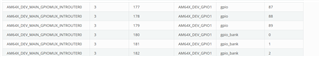
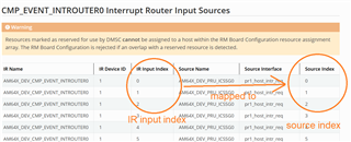
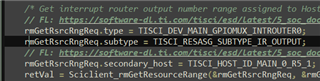
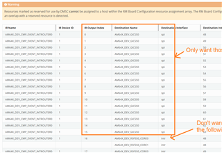
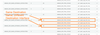
https://software-dl.ti.com/tisci/esd/latest/5_soc_doc/am64x/interrupt_cfg.html#main-gpiomux-introuter0-interrupt-router-input-sources
regarding that for GPIO module GPIO0 the source index numbers for the single pins go from 0 to 89. And then GPIO module GPIO1 source index numbers start at 0 again, while the interrupt router output is at 90,
which would fit to the example value of source index.
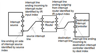
Here I am not sure if what is provided in the TISCI message as source index is actually the interrupt routers input index, which would match the description here
https://software-dl.ti.com/tisci/esd/latest/2_tisci_msgs/rm/rm_irq.html#irq-route-set-message-parameters
of the "Interrupt Router Mux Configuration" but then again source ID and destination ID in the example are not the INTRs device ID as requested in the comments for the "Interrupt Router Mux Configuration"
but the device ID of the source and the destination.
Though when looking at the interrupt path tree traversion in drivers/sciclinet/sciclient_rq_irq.c it seems that it does not matter which one to take as long as the connections between input and source or output and destination are just singular without branching, which they always are.
Anyway to get to my questions:
The numbering with base and pin number of the source index in the examples is clearly due to pins being numbered in the same way no matter which module they are in.
1. Maybe this is just a problem of the naming in the example but to me TISCI_BANK_SRC_IDX_BASE_GPIO1 appears quite confusing.
It suggests that it is the source index base for the bank, while actually it is the base for the GPIO module.,
When looking again at
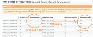
https://software-dl.ti.com/tisci/esd/latest/5_soc_doc/am64x/interrupt_cfg.html#main-gpiomux-introuter0-interrupt-router-input-sources
the bank interrupt router input index numbers for GPIO1 start with 180 and not 90.
Maybe there is some intended meaning in the name that I simply didn't get.
If that is the case, please enlighten me. If not could you maybe update the documentation please so that it is more clear?
2. Additionally adding to the confusion from question 2 in addition to the weird naming of the base number GPIO_GET_BANK_INDEX(GPIO_PUSH_BUTTON_PIN) is added,
which is the bank index of the GPIO bank holding the PUSH_BUTTON pin.
To me this suggests together with the naming for the base, that originally the example was ment for a bank interrupt and not a pin interrupt.
And then somebody remodelled it to a pin interrupt, changed the base number to the base of GPIO module GPIO1 for the single pin index numbers,
but forgot to change the name and also left GPIO_GET_BANK_INDEX(GPIO_PUSH_BUTTON_PIN) in, while the correct term would have been something like either
#define TISCI_BANK_SRC_IDX_BASE_GPIO1 180

TISCI_BANK_SRC_IDX_BASE_GPIO1 + GPIO_GET_BANK_INDEX(GPIO_PUSH_BUTTON_PIN);
for a bank interrupt,
or for a single pin
#define TISCI_PIN_SRC_IDX_BASE_GPIO1 90

TISCI_PIN_SRC_IDX_BASE_GPIO1 + GPIO_PUSH_BUTTON_PIN;
Please correct me if I am wrong.
Thank you for your time and trouble.
Best regards
Philip.