Other Parts Discussed in Thread: SYSCONFIG
Hi,
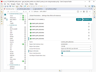
I am currently working with the AM2343 and its SDK. In my project, we want to interface a DAC and an ADC from the GPMC peripheral (which could be eventually drive by a DMA). We guessed this could be possible since both the DAC and ADC have a parallel interface that is really close to a SRAM. There is no driver in the SDK for the GPMC yet and I have seen that the driver are scheduled to be done this June. I cannot wait for that : my projet has a really close deadline. So, I am trying to write the driver by myself. So far I have been able to set the GPMC register, but when I try to write something to the GPMC, the code falls in the HwiP_data_abort_handler handler. I am not quite sure how to write or read something from the GPMC... There is the 0x05000000 address in the Table 2-1 that is related to GPMC0_DATA region. So I guess this is the region that is linked to the GPMC? Is there something else I need to do to activate those addresses? Is the use of the GPMC for my purpose a good idea? In definitive, I just want to read and write 16 bits data to a parallel bus at a speed of around 125MSps...
Here is my code :
typedef struct
{
    uint32_t REVISION;          // 0x0000
    uint32_t RESERVED_0[3];     // 0x0004
    uint32_t SYSCONFIG;         // 0x0010
    uint32_t SYSSTATUS;         // 0x0014
    uint32_t IRQSTATUS;         // 0x0018
    uint32_t IRQENABLE;         // 0x001C
    uint32_t RESERVED_1[8];     // 0x0020
    uint32_t TIMEOUT_CONTROL;   // 0x0040
    uint32_t ERR_ADDR;          // 0x0044
    uint32_t ERR_TYPE;          // 0x0048
    uint32_t RESERVED_6;        // 0x004C
    uint32_t CONFIG;            // 0x0050
    uint32_t STATUS;            // 0x0054
    uint64_t RESERVED_7;        // 0x0058
    struct
    {
        uint32_t CONFIG1;         // 0x0060
        uint32_t CONFIG2;         // 0x0064
        uint32_t CONFIG3;         // 0x0068
        uint32_t CONFIG4;         // 0x006C
        uint32_t CONFIG5;         // 0x0070
        uint32_t CONFIG6;         // 0x0074
        uint32_t CONFIG7;         // 0x0078
        uint32_t NAND_COMMAND;    // 0x007C
        uint32_t NAND_ADDRESS;    // 0x0080
        uint32_t NAND_DATA;       // 0x0084
        uint64_t RESERVED_0;      // 0x0088
    } UNIT[4];                    // 0x0090
    uint32_t RESERVED_2[48];    // 0x0120
    uint32_t PREFETCH_CONFIG1;  // 0x01E0
    uint32_t PREFETCH_CONFIG2;  // 0x01E4
    uint32_t PREFETCH_CONTROL;  // 0x01E8
    uint32_t PREFETCH_STATUS;   // 0x01EC
} GPMC_Type;

#define GPMC0_BASE (0x3B000000)
#define GPMC0 ((GPMC_Type *) GPMC0_BASE)


static Pinmux_PerCfg_t gpmcPinConfig[] = {
        {PIN_GPMC0_CLK, ( PIN_MODE(0) )},
        {PIN_GPMC0_AD0, ( PIN_MODE(0) | PIN_INPUT_ENABLE )},
        {PIN_GPMC0_AD1, ( PIN_MODE(0) | PIN_INPUT_ENABLE )},
        {PIN_GPMC0_AD2, ( PIN_MODE(0) | PIN_INPUT_ENABLE )},
        {PIN_GPMC0_AD3, ( PIN_MODE(0) | PIN_INPUT_ENABLE )},
        {PIN_GPMC0_AD4, ( PIN_MODE(0) | PIN_INPUT_ENABLE )},
        {PIN_GPMC0_AD5, ( PIN_MODE(0) | PIN_INPUT_ENABLE )},
        {PIN_GPMC0_AD6, ( PIN_MODE(0) | PIN_INPUT_ENABLE )},
        {PIN_GPMC0_AD7, ( PIN_MODE(0) | PIN_INPUT_ENABLE )},
        {PIN_GPMC0_AD8, ( PIN_MODE(0) | PIN_INPUT_ENABLE )},
        {PIN_GPMC0_AD9, ( PIN_MODE(0) | PIN_INPUT_ENABLE )},
        {PIN_GPMC0_AD10, ( PIN_MODE(0) | PIN_INPUT_ENABLE )},
        {PIN_GPMC0_AD11, ( PIN_MODE(0) | PIN_INPUT_ENABLE )},
        {PIN_GPMC0_AD12, ( PIN_MODE(0) | PIN_INPUT_ENABLE )},
        {PIN_GPMC0_AD13, ( PIN_MODE(0) | PIN_INPUT_ENABLE )},
        {PIN_GPMC0_AD14, ( PIN_MODE(0) | PIN_INPUT_ENABLE )},
        {PIN_GPMC0_AD15, ( PIN_MODE(0) | PIN_INPUT_ENABLE )},
        {PIN_GPMC0_WAIT0, ( PIN_MODE(0) | PIN_INPUT_ENABLE )},
        {PIN_GPMC0_CSN0, ( PIN_MODE(0) )},
        {PIN_GPMC0_CSN1, ( PIN_MODE(0) )},
        { PINMUX_END, PINMUX_END }, };

void GPMC_Init()
{
    // Init the clock
    SOC_moduleClockEnable(TISCI_DEV_GPMC0, 1);

    // Init the GPMC Pin
    Pinmux_config(gpmcPinConfig, PINMUX_DOMAIN_ID_MAIN);

    // Reset the GPMC
    // ??

    // Init the GPMC 0 for the DAC
    GPMC0->UNIT[0].CONFIG1 = (1 << 28)  // Enable the write multiple access
            | (1 << 27)     // Select the write synchronous
            | (1 << 24)     // Set the device burst page of 16 words
            | (1 << 12);    // Set the device size at 16 bits

    // Try a write command
    while(1)
    {
        unsigned short *addr = (unsigned short*) 0x50000000;
        (*addr) = 0x0003;


    }
}
Thank you,
Leo