This thread has been locked.

If you have a related question, please click the "Ask a related question" button in the top right corner. The newly created question will be automatically linked to this question.

TM4C129XNCZAD: Hardware CRC error when using optimizations

Part Number: TM4C129XNCZAD

Hi,

We've been recently encountering an unexpected issue regarding the use of the hardware CRC.

Our code is quite simple and has been tested without any trouble....

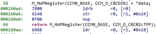
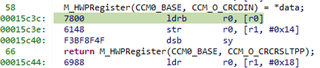
	// Write the control register with the configuration
	M_HWPRegister(CCM0_BASE, CCM_O_CRCCTRL) = (CRC_CFG_INIT_1 |
	                                           CRC_CFG_SIZE_8BIT |
	                                           CRC_CFG_TYPE_P1021);

	// Feed the CRC module with data
	while (length-- != 0u)
	{
		M_HWPRegister(CCM0_BASE, CCM_O_CRCDIN) = *bytes++;
	}

	// Return post processed value
	return M_HWPRegister(CCM0_BASE, CCM_O_CRCRSLTPP);

.... until we applied the -O2 optimization.

Once the -O2 optimization was applied, we check the assembly code which is correct but the calculated CRC was different when running the code and when going step by step in assembly.

After further investigation, the CRC was correct when going by step but when running the code, the returned CRC was the one of the length-1 first bytes of the array and in this case, when halting the processor, the correct CRC was contained in the CCM0 module register, contrary to what was returned by the function.

Quotes from the datasheet:

" CRCs are computed combinatorially in one clock."
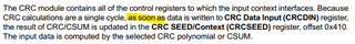
" Because CRC calculations are a single cycle, as soon as data is written to CRC Data Input (CRCDIN) register, the result of CRC/CSUM is updated in the CRC SEED/Context (CRCSEED) register, offset 0x410."

Is this incorrect? Is there an undocumented timing when reading the CRC Post Processing Result (CRCRSLTPP) register? How can a CRC calculation take one cycle and not a XOR or a bit reverse?

We added a NOP instruction between the last written byte and the read of the post processing result and it seems to work. However, as we are working in a medical device company, this is an unacceptable patch without providing any additional information to justify it.

Best regards,

Matthieu Tardivon

  • Hi Matthieu,

      Reading the datasheet for CRC module operation, I'm not sure why you are not reading the CRC checksum from the CRCSEED register. In your initialization, I don't see you select any post-processing feature. You only select CRC_CFG_INIT_1 | CRC_CFG_SIZE_8BIT |CRC_CFG_TYPE_P1021. What if you read the CRCSEED register instead of CRCRSLTPP? Do you see the correct checksum result or it is also affected by -o2 optimization?

    12.2.1 CRC Initialization and Configuration
    The CRC engine works in push through mode, which means it works on streaming data. This section
    describes the steps for initializing the CRC module:


    1. Enable the CRC by setting the R0 bit in the CRC Module (RCGCCM) register, System Control
    offset 0x674.


    2. Configure the desired CRC data size, bit order, endian configuration and CRC type by
    programming the CRC Control (CRCCTRL) register, offset 0x400.


    3. If the CRC value has not been initialized to all 0s or all 1s using the INIT field in the CRCCTRL
    register, program the initial value in the CRC SEED/Context (CRCSEED) register, offset 0x410.


    4. Repeatedly write the DATAIN field in the CRC Data Input (CRCDIN) register, offset 0x414. If
    the SIZE bit in the CRCCTRL register is set to select byte, the CRC engine operates in byte
    mode and only the least significant byte is used for CRC calculation.


    5. When CRC is finished, read the CRCSEED register for the final result. If using post-processing,
    the raw CRC result is stored in the CRCSEED register and the final, post-processed result can
    be read from the CRC Post-Processing Result (CRCRSLTPP) register, offset 0x418.
    Post-processing options are selectable through the OBR and OLNV bits of the CRCCTRL register

  • Is this incorrect? Is there an undocumented timing when reading the CRC Post Processing Result (CRCRSLTPP) register? How can a CRC calculation take one cycle and not a XOR or a bit reverse?
    We added a NOP instruction between the last written byte and the read of the post processing result and it seems to work.

     I don't have visibility to the actual circuity of the CRC module. It is possible that the computed checksum is stored to the CRCSEED register first and then go through the post-processing before capturing the post-processed data into CRCRSLTPP register. This can result in an one cycle difference between CRCSEED and CRCRSLTPP. I'm not an compiler expert. I think -o2 can change the order of the sequence. Putting a NOP is a right thing to do to.

  • I tried replacing CCM_O_CRCRSLTPP by CCM_O_CRCSEED and I observe the same behavior. This therefore suggests multiple clock cycles to perform the operation contrary to what is mentioned in the datasheet. Can you check that on your side ? It is important for us to know how does it take before reading getting the correct value within the register.

    Also, the reason we checked the post processing register rather than the seed register was to have a better portable code so that if we decide to change the configuration within the control register, the rest of the calculation remains the same.

  • Hi,

      I don't think it takes multiple cycles for CRC to calculate the checksum. It does look like the optimizer is re-arranging the order of read. Can you show the assembly code?

      Please also find this below article about memory barrier. As it is described, Cortex-M4F is based on Armv7E-M architecture allows processor for out of order memory operation. As far as the processor is concerned, the write to CRCDIN and the read from CRCRSLTPP are two different memory transfers. The read does not depend on the write to complete. Adding a memory barrier instruction or like what you did with a NOP is a correct remedy in my opinion. Please also try to declare the variable volatile. 

    https://www.sciencedirect.com/topics/engineering/memory-barrier-instruction

  • Hi,

    The register access is already declared as volatile:

    //! \brief Access a peripheral hardware register
    #define M_HWPRegister(peripheral, reg)     (*(reinterpret_cast<volatile uint32*>(static_cast<uint32>(peripheral) + static_cast<uint32>(reg))))

    Code is not re-arranged and instructions are executed in the correct order as you can check in the screenshot below. You can even notice that a BNE instruction is executed between the STR to CRCDIN register and the LDR to CRCSEED register. As adding a NOP instruction added between the BNE and LDR instruction seems to solve the problem, a DSB instruction will most likely work even better but this is still in contradiction with what is mentioned in the datasheet:

    To correctly solve a problem, it is needed to understand it first, this is why we would like a justified hardware explanation to ensure that this is correct fix to perform.

    Best regards,

    Matthieu Tardivon

  • Hi Matthieu,

      As I mentioned in my earlier reply, I have no visibility into the design as the design was done quite some time ago. With that said, I looked at TivaWare API CRCDataProcess() on how it returns the processed data, it is evident that it calls CRCResultRead() at the end. By calling CRCResultRead, it clearly will introduce delay with similar effect to NOPs. Perhaps, it was done intentionally during the API development when they encountered the same issue that you are facing and therefore making another function call to delay the read of the checksum.  I think if you were to use TivaWare to read out the data, you would not encounter the issue. Can you try to use TivaWare? If you still want to stay with your own code (DRM style), adding NOP is the right thing to do.


    uint32_t
    CRCDataProcess(uint32_t ui32Base, uint32_t *pui32DataIn,
                   uint32_t ui32DataLength, bool bPPResult)
    {
        uint8_t *pui8DataIn;
    
        //
        // Check the arguments.
        //
        ASSERT(ui32Base == CCM0_BASE);
    
        //
        // See if the CRC is operating in 8-bit or 32-bit mode.
        //
        if(HWREG(ui32Base + CCM_O_CRCCTRL) & CCM_CRCCTRL_SIZE)
        {
            //
            // The CRC is operating in 8-bit mode, so create an 8-bit pointer to
            // the data.
            //
            pui8DataIn = (uint8_t *)pui32DataIn;
    
            //
            // Loop through the input data.
            //
            while(ui32DataLength--)
            {
                //
                // Write the next data byte.
                //
                HWREG(ui32Base + CCM_O_CRCDIN) = *pui8DataIn++;
            }
        }
        else
        {
            //
            // The CRC is operating in 32-bit mode, so loop through the input data.
            //
            while(ui32DataLength--)
            {
                //
                // Write the next data word.
                //
                HWREG(ui32Base + CCM_O_CRCDIN) = *pui32DataIn++;
            }
        }
    
        //
        // Return the result.
        //
        return(CRCResultRead(ui32Base, bPPResult));

  • Hi,

    I am sorry but I am really disappointed by your answer. This is a first time I receive such a vague answer for someone who works in THE company that manufactures the MCU.

    "I have no visibility into the design as the design was done quite some time ago"
    You work in the company, if you don't then, who does? I have been working with your products and discussing with you guys for a while and this is the first time my confidence gets shaken.

    "Perhaps, it was done intentionally during the API development"
    I work in a medical device company, "perhaps" is not acceptable. Our development must be done on a solid basis, we need data to do our job correctly and professionally.

    "If you still want to stay with your own code (DRM style), adding NOP is the right thing to do"
    Actually NO it is not the right thing to do, after doing some investigation and modifying my code in order to have a minimum of assembly instruction:

    This fails:

    This works:

    Conclusion, adding a DSB instruction SEEMS to be the right thing to do. At least with this test, as I minimized the number of instructions, it should be enough to justify the workaround in our documentation. But once again, this is the perfect example that assumptions are not enough to solve an issue and I expect from TI to be professional, to perform a clear HW analysis and provide a documentation update which specifies with certitude what is the right thing to do.

    Best regards,
    Matthieu Tardivon

  • Hi Matthieu,

      I'm sorry that I cannot provide an answer you are looking for. The silicon design of this MCU was done close to 10 years ago. The design database base for the silicon was already on tape archive. Even if the design database can be retrieved, I'm not even sure what will be the hurdles to open and simulate the database as EDA tools do change frequency in a span of 10 years. Lastly, I'm an application engineer who picked up this MCU support in the last few years and there are no longer design engineers around with the knowledge for this MCU who can simulate the database. I understand my answer may not be taken by you but unfortunately, this is the best explanation I can give.  

  • Hi Matthieu,

    "I have no visibility into the design as the design was done quite some time ago"
    You work in the company, if you don't then, who does? I have been working with your products and discussing with you guys for a while and this is the first time my confidence gets shaken.

    What Charles stated regarding the designs being in archive is the unfortunate truth here. It is frustrating for us at times like these as well because we want to be able to provide better answers for questions like this. I can understand your concerns clearly.

    "Perhaps, it was done intentionally during the API development"
    I work in a medical device company, "perhaps" is not acceptable. Our development must be done on a solid basis, we need data to do our job correctly and professionally.

    Let's break this up into two aspects here.

    Aspect #1: The intent of the TivaWare API design

    We are not positive on why the TivaWare API was written to make the additional TivaWare API call in the return statement, but it is clearly a departure from how TivaWare is traditionally handled. Hence we suspect but cannot confirm that this was an intentional adjustment to avoid the issue you are seeing. So the 'perhaps' statement is purely regarding past development.

    Aspect #2: The issue at hand and the functionality of the TivaWare API

    What you have presented is a unique case to us. We have not had prior questions regarding this exactly behavior before and no one using the TivaWare API has had an issue like this.

    The issue from what we can see seems to stem from how you are developing your own code at a DRM level. The mismatch between the steps you are taking vs the steps our TivaWare API took is therefore likely introducing this issue unless you are (unlikely) the only customer to use this feature in the past 5+ years.

    Based on the results you are getting with your various tests, it is very clear that additional cycles are needed to get the CRC data updated. Yes, that is a departure from the datasheet, but right now all evidence points to the additional cycles being a requirement to be able to get the data.

    And I do say 'cycles' intentionally as it is clear that a single NOP alone was not enough. The TivaWare API call used introduces multiple cycles and so a single NOP does not fully replicate what is occurring with the proven API. The DSB instruction is working better as it is has the potential to wait additional cycles rather than just a single cycle.

    What you should test as well is using three to five NOPs. I did an assembly breakdown of the proven TivaWare API and it adds minimum 5 additional cycles between the BNE and LDR instructions. What is not clear is how reliable DSB will be to always introduce enough delay - if you want to use it, then make sure to validate that. Otherwise I would recommend ensuring more than 1 cycle is delayed. Minimum of five has been proven to work via TivaWare API but I strongly suspect that three cycles is sufficient based on both my years of experience and the results presented by your evaluations. You could certainly just test the robustness of DSB or even two NOPs but my official recommendation is minimum three cycles of delay and validate that it works properly moving forward.

    To get back to the topic of your confidence in this proposal...

    When looking that the TivaWare API:

    1. Adds additional cycles
    2. Is designed different than other APIs in how it introduces extra cycles
    3. Has not been reported to have issues

    Plus the data you've presented that adding cycles works at an assembly level, it is clear to use as device experts that the datasheet is incorrect regarding the 'as soon as' statement and you will need to introduce additional cycles to ensure you get the result. 

    While we don't have the capability to access the design to verify this, I would not say this is a 'perhaps' you need more cycles. It is abundantly clear that it is required and mismatches the datasheet based on the detailed investigation you have done. Therefore our technical recommendations based on our knowledge of the devices are:

    1. If possible, use the proven TivaWare API.
    2. If not, ensure minimum of three cycles are added in between BNE and LDR to allow the result to appear in CRC Seed/Context register and validate that adjustment. To replicate TivaWare API delays, a minimum of five cycles of delay would be needed.

    I understand that is not the same level of certainty as verifying at a design level, but my intent here is for this added explanation gives you more confidence about the proposed solution.

    Best Regards,
    Ralph Jacobi

  • Hi Ralph,

    Thank you for your detailed answer. I understand your frustration if you can't access any live version of the latest design on a running server to do your job, this is a pity and I hope your management will take that matter into account in the future so that it can benefit your team and the customer in the end.

    Regarding the technicalities, what I suppose is that the CRC HW calculation is done through a combination of mostly asynchronous gates and one stage of synchronous gates/flip-flops, which would explain the "single cycle" and "computed combinatorially in one clock" statements in the datasheet. The limitation would therefore come from what is stated in Charles's link: "However, due to the fact that the processor has a write buffer (as mentioned in section 6.9), a data write that takes multiple clock cycles might happen in parallel with execution of subsequent operations.". This also why I believe the use of a DSB instruction is probably the most robust solution and we will stick to it as it should be easily testable. If we encounter some similar issues again, we'll follow your advice to behave like TivaWare and we'll add the NOP instructions.

    Best regards,
    Matthieu Tardivon