


Hi,
I have a TPR12 EVM. I am trying to communicate with a microchip cryptoauth EVM using I2C. The TPR12 board is configured to be in master mode and the microchip EVM is in slave mode. Theoretically, my communication should look as following:
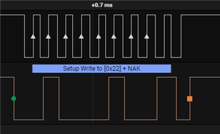
- Send 0x00 (data) to the address 0x00. I should receive a NACK for this address and therefore the data bytes 0x00 should never be sent. This is done to wake the device up.
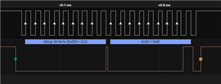
- Next, I send a data array (0x03, 0x07, 0x30, 0x00, 0x00, 0x00, 0x03, 0x5D) to the device address (0x36). I should see an ACK for this. This is done to receive the silicon revision of the device.
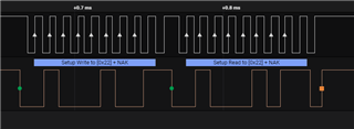
- Lastly, I write 0x00 to the address 0x36 and start reading 7 bytes of silicon revision data from the microchip.
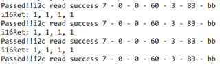
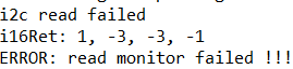
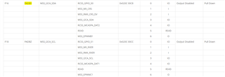
However, when I try to run this and get the return values from the function I2C_transfer() on TPR12, I get the error code I2C_STS_ERR_NO_ACK (-3) for all stages. The weird part is, it is still receiving the correct data as shown in the screenshot.

The silicon revision is 7-0-0-60-3-83-bb.
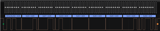
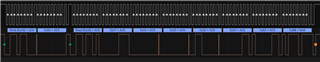
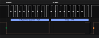
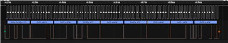
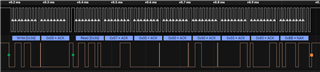
I also used a logic analyzer to see what's going on at every step.
On step 1, it sends the device address 0x00 and receives a positive acknowledgement (it should not) and sends the data 0x00 receiving a negative acknowledgement. This still wakes the device up.
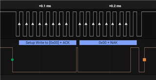
On step 2, it sends the data buffer to 0x36 address of the device and microchip sends an ACK. However, the TPR12 still says it didn't receive an a acknowledgement as it gives -3 error code.
On the last step, it writes 0x00 to the address 0x36 and receives the data from the microchip but does not give an ACK back on the last byte.
I am not sure why it is behaving like this. Can someone with more insight on this help me out please?
