This thread has been locked.

If you have a related question, please click the "Ask a related question" button in the top right corner. The newly created question will be automatically linked to this question.

TMS570LC4357: Is MPU same as NMPU?

Part Number: TMS570LC4357

Hi all:

   1. I find NMPU(new memory protection unit) in LC4357 datasheet (chapter 11 - system emory protection unit). Also when I read "Cortex-R5 Technical reference manual" , I find  " chapter 7 - Memory protect unit" is very similar to NMPU.

   Are they same? if not what difference?

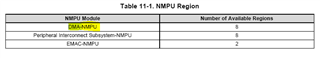
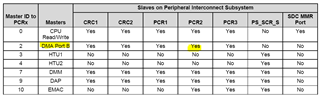
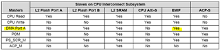
   2. I also find there is a build-in MPU in DMA.  According to the Figure 2-1 in the TRM, I am confused about built-in mpu, NMPU, and MPU. In my mind, when DMA accesss scr, it should have NMPU and MPU; when DMA access pcr, it only has one NMPU or build-in mpu?

  3. In MPU, for the mpu Region Access Permission, I understand strongly odered, shareable, non shareable but what are the execution and no execution?


Best Wish

Li

  • Are they same? if not what difference?

    They are similar, but different. The MPU is for CPU, but NMPU is for other master such as DMA, EMAC, etc.

    2. In MPU, for the mpu Region Access Permission, I understand strongly odered, shareable, non shareable but what are the execution and no execution?


    Each MPU region can be given no access, read-only access, or read/write access permissions, and each region can also be marked as eXecute Never (XN) to prevent instructions being fetched from that region.

    Any address in an MPU region with device or strongly-ordered memory type attributes is implicitly given execute-never (XN) permissions.

  • thank you QJ;

     I also find there is a build-in MPU in DMA.  According to the Figure 2-1 in the TRM, I am confused about built-in mpu, NMPU, and MPU. In my mind, when DMA accesss scr, it should have NMPU and MPU; when DMA access pcr, it only has one NMPU or build-in mpu?

  • it only has one NMPU or build-in mpu?

    As I said that the NMPU is for DMA/EMAC/Peripheral Interconnect Subsystem, and MPU is for CPU only. 

    Up to 8 memory protection regions for DMA:

    To configure DMA NMPU, the base address for the NMPU control registers is 0xFFFF1A00. 

  • Thank you QJ. The last question, If I use DMA to access data (in RAM on chip) through dma port_a , do I have to configure NMPU?

    If I do not configure NMPU which means I can not access data in ram through dma_port a?

    Or what about access data in ram through dma_port b?

  • You don't have to enable and configure the NMPU.

    After the reset, the NMPU is disabled by default. If NMPUis disabled, no filtering (NMPU permission, etc) will be done on the bus.

  • Thank you QJ. I have known a little about the NMPU and "If I use DMA to access data (in RAM on chip) through dma port_a", is the dma port_a the only way for DMA to access on-chip ram?

  • Yes, DMA accesses L2 RAM through the DMA Port A, and CPU interconnect.

  • Thank you QJ. 

    I wonder the external memory the EMIF SDRAM which address range  is "0x80000000 -- 0x9FFFFFFF"  belongs to  EMIF Slaves of "Peripheral Interconnect Subsystem" or EMIF on CPU?

  • All bus masters (DMA, CPU, etc) have a point to point connection to the EMIF slave through CPU interconnect rather than Peripheral Interconnect.

  • So you mean if I access SDRAM through DMA, the way should be "DMA port_a" -> "CPU Interconnect Subsystem"->"EMIF" rather than "DMA port_b"->"pcr2"->"EMIF Slave".

    In my project ,I have a WtBuf[256] and RdBuf[256] which defined in SDRAM, when SPI receive data from SD card, the DMA will move data from "SPI_RX register" to RdBuf[256]; When I fill the WtBuf, the DMA will move the data to "SPI_TX register."

    However, when I define WtBuf[256] and RdBuf[256] in SRAM rather SDRAM, the DMA can not access these two buffers; In my mind, maybe something wrong with configuration of DMA.

  • "DMA port_b"->"pcr2"->"EMIF Slave".

    DMA port_b is used to access the register rather than the EMIF memory.

    when I define WtBuf[256] and RdBuf[256] in SRAM rather SDRAM, the DMA can not access these two buffers;

    I don't see this kind of issue before. DMA can access EMIF memory (SDRAM, or SRAM).

  • "I define WtBuf[256] and RdBuf[256] in SRAM rather SDRAM, the DMA can not access these two buffers;"

    Here the SRAM means the on chip ram 512kB which range is "0x08000000 - 0x0807FFFF".

    I have MPUsetting for CPU. The rule for on-chip RAM is same as external SDRAM which is " (U32)MPU_PRIV_RW_USER_RO_NOEXEC | (U32)MPU_NORMAL_OIWBNOWA_SHARED"

  • Please use my example to transfer data from one location in sram to another location in sram:

    /** @file HL_sys_main.c 
    *   @brief Application main file
    *   @date 11-Dec-2018
    *   @version 04.07.01
    *
    *   This file contains an empty main function,
    *   which can be used for the application.
    */
    
    /* 
    * Copyright (C) 2009-2018 Texas Instruments Incorporated - www.ti.com  
    * 
    * 
    *  Redistribution and use in source and binary forms, with or without 
    *  modification, are permitted provided that the following conditions 
    *  are met:
    *
    *    Redistributions of source code must retain the above copyright 
    *    notice, this list of conditions and the following disclaimer.
    *
    *    Redistributions in binary form must reproduce the above copyright
    *    notice, this list of conditions and the following disclaimer in the 
    *    documentation and/or other materials provided with the   
    *    distribution.
    *
    *    Neither the name of Texas Instruments Incorporated nor the names of
    *    its contributors may be used to endorse or promote products derived
    *    from this software without specific prior written permission.
    *
    *  THIS SOFTWARE IS PROVIDED BY THE COPYRIGHT HOLDERS AND CONTRIBUTORS 
    *  "AS IS" AND ANY EXPRESS OR IMPLIED WARRANTIES, INCLUDING, BUT NOT 
    *  LIMITED TO, THE IMPLIED WARRANTIES OF MERCHANTABILITY AND FITNESS FOR
    *  A PARTICULAR PURPOSE ARE DISCLAIMED. IN NO EVENT SHALL THE COPYRIGHT 
    *  OWNER OR CONTRIBUTORS BE LIABLE FOR ANY DIRECT, INDIRECT, INCIDENTAL, 
    *  SPECIAL, EXEMPLARY, OR CONSEQUENTIAL DAMAGES (INCLUDING, BUT NOT 
    *  LIMITED TO, PROCUREMENT OF SUBSTITUTE GOODS OR SERVICES; LOSS OF USE,
    *  DATA, OR PROFITS; OR BUSINESS INTERRUPTION) HOWEVER CAUSED AND ON ANY
    *  THEORY OF LIABILITY, WHETHER IN CONTRACT, STRICT LIABILITY, OR TORT 
    *  (INCLUDING NEGLIGENCE OR OTHERWISE) ARISING IN ANY WAY OUT OF THE USE 
    *  OF THIS SOFTWARE, EVEN IF ADVISED OF THE POSSIBILITY OF SUCH DAMAGE.
    *
    */
    
    
    /* USER CODE BEGIN (0) */
    /* USER CODE END */
    
    /* Include Files */
    
    #include "HL_sys_common.h"
    
    /* USER CODE BEGIN (1) */
    //#include "HL_emif.h"
    #include "HL_sys_dma.h"
    #include "HL_sys_core.h"
    #include "HL_gio.h"
    #include "HL_pinmux.h"
    #include "HL_esm.h"
    
    
    /* example data Pattern configuration */
    #define E_COUNT      8   /*64, Element count*/
    #define F_COUNT      32    /*16, Frame count*/
    #define D_SIZE      E_COUNT * F_COUNT
    
    void loadDataPattern(uint32 psize, uint32* pptr, uint32 pattern);
    
    
    #pragma SET_DATA_SECTION(".sharedRAM")
    uint32 TXDATA_RAM0[D_SIZE];         /* transmit buffer in sys ram */
    uint32 RXDATA_RAM0[D_SIZE]= {0};    /* receive  buffer in sys ram */
    
    uint32 TXDATA_RAM1[D_SIZE];         /* transmit buffer in sys ram */
    uint32 RXDATA_RAM1[D_SIZE]= {0};    /* receive  buffer in sys ram */
    
    g_dmaCTRL g_dmaCTRLPKT1, g_dmaCTRLPKT2;  /* dma control packet configuration stack */
    
    #pragma SET_DATA_SECTION()
    
    /* USER CODE END */
    
    /** @fn void main(void)
    *   @brief Application main function
    *   @note This function is empty by default.
    *
    *   This function is called after startup.
    *   The user can use this function to implement the application.
    */
    
    /* USER CODE BEGIN (2) */
    unsigned int Channel0_HBC_Flag;
    unsigned int Channel1_HBC_Flag;
    
    /* USER CODE END */
    
    int main(void)
    {
    /* USER CODE BEGIN (3) */
        /* enable IRQ interrupt */
        /*clear ESM error*/
        uint16 i, j=0;
    
        gioInit();
    
        _enable_IRQ();
    
        Channel0_HBC_Flag = 0;
        Channel0_HBC_Flag = 1;
    
        //dmaREG->PTCRL = 0x03 | 0x1 << 3 | 0x1 << 18;  /* prority scheme: rotation*/
    
        /* - creating a data chunk in system ram to start with ... */
        loadDataPattern(D_SIZE, &TXDATA_RAM0[0], 0x5A5A5A5A);
        loadDataPattern(D_SIZE, &TXDATA_RAM1[0], 0x5B5B5B5B);
    
       /* - configuring dma control packets   */
       g_dmaCTRLPKT1.SADD      = (uint32)TXDATA_RAM0;    /* source address             */
       //g_dmaCTRLPKT1.DADD      = (uint32)(0x80000000);  //(0x08078000);    /* destination address; SDRAM       */
       g_dmaCTRLPKT1.DADD      = (uint32)RXDATA_RAM0;  //(0x08078000);    /* destination address; SDRAM       */
       g_dmaCTRLPKT1.CHCTRL    = 0;                 /* channel control            */
       g_dmaCTRLPKT1.FRCNT     = F_COUNT;                 /* frame count                */
       g_dmaCTRLPKT1.ELCNT     = E_COUNT;            /* element count              */
       g_dmaCTRLPKT1.ELDOFFSET = 0;                 /* element destination offset */
       g_dmaCTRLPKT1.ELSOFFSET = 0;                 /* element destination offset */
       g_dmaCTRLPKT1.FRDOFFSET = 0;                 /* frame destination offset   */
       g_dmaCTRLPKT1.FRSOFFSET = 0;                 /* frame destination offset   */
       g_dmaCTRLPKT1.PORTASGN  = PORTA_READ_PORTA_WRITE;
       g_dmaCTRLPKT1.RDSIZE    = ACCESS_32_BIT;     /* read size                  */
       g_dmaCTRLPKT1.WRSIZE    = ACCESS_32_BIT;     /* write size                 */
       g_dmaCTRLPKT1.TTYPE     = FRAME_TRANSFER ;   /* transfer type              */
       g_dmaCTRLPKT1.ADDMODERD = ADDR_INC1;         /* address mode read          */
       g_dmaCTRLPKT1.ADDMODEWR = ADDR_INC1;        /* address mode write         */
       g_dmaCTRLPKT1.AUTOINIT  = AUTOINIT_ON;       /* autoinit                   */
    
    
       //g_dmaCTRLPKT2.SADD      = (uint32)(0x80001000);  //0x08076000);    /* source address */
       g_dmaCTRLPKT2.SADD      = (uint32)TXDATA_RAM1;  //0x08076000);    /* source address */
       g_dmaCTRLPKT2.DADD      = (uint32)RXDATA_RAM1;       /* destination  address       */
       g_dmaCTRLPKT2.CHCTRL    = 0;                 /* channel control            */
       g_dmaCTRLPKT2.FRCNT     = F_COUNT;                 /* frame count                */
       g_dmaCTRLPKT2.ELCNT     = E_COUNT;             /* element count              */
       g_dmaCTRLPKT2.ELDOFFSET = 0;                 /* element destination offset */
       g_dmaCTRLPKT2.ELSOFFSET = 0;                 /* element destination offset */
       g_dmaCTRLPKT2.FRDOFFSET = 0;                 /* frame destination offset   */
       g_dmaCTRLPKT2.FRSOFFSET = 0;                 /* frame destination offset   */
       g_dmaCTRLPKT2.PORTASGN  = PORTA_READ_PORTA_WRITE;
       g_dmaCTRLPKT2.RDSIZE    = ACCESS_32_BIT;     /* read size                  */
       g_dmaCTRLPKT2.WRSIZE    = ACCESS_32_BIT;     /* write size                 */
       g_dmaCTRLPKT2.TTYPE     = FRAME_TRANSFER ;   /* transfer type              */
       g_dmaCTRLPKT2.ADDMODERD = ADDR_INC1;         /* address mode read          */
       g_dmaCTRLPKT2.ADDMODEWR = ADDR_INC1;       /* address mode write         */
       g_dmaCTRLPKT2.AUTOINIT  = AUTOINIT_ON;       /* autoinit                   */
    
       /* - setting dma control packets */
       dmaSetCtrlPacket(DMA_CH1, g_dmaCTRLPKT1);  //tx
       dmaSetCtrlPacket(DMA_CH0, g_dmaCTRLPKT2);  //rx
    
       /* - setting the dma channel to trigger on h/w request */
       dmaSetChEnable(DMA_CH1, DMA_SW);
       dmaSetChEnable(DMA_CH0, DMA_SW);
    
       /* Enable Block Transfer Complete interrupt for the receive after transfer complete */
       dmaEnableInterrupt(DMA_CH0, FTC, DMA_INTA);
       dmaEnableInterrupt(DMA_CH1, FTC, DMA_INTA);
    
       dmaEnable();
    
       for(i=1; i<F_COUNT; i++)
       {
           dmaSetChEnable(DMA_CH1, DMA_SW);
           dmaSetChEnable(DMA_CH0, DMA_SW);
           j = i;
       }
    
       while(1); /* loop forever */
    
    /* USER CODE END */
    
        return 0;
    }
    
    
    /* USER CODE BEGIN (4) */
    
    /** void loadDataPattern(uint32 psize, uint16* pptr)
    */
    void loadDataPattern(uint32 psize, uint32* pptr, uint32 pattern)
    {
        int i;
        for(i=0;i<psize;i++)
        {
            *(pptr++) = pattern + i;
        }
     }
    
    
    /**************************************************************************//**
     *  DMA Interrupt
     *****************************************************************************/
    void dmaGroupANotification(dmaInterrupt_t inttype, uint32 channel)
    {
    /*  enter user code between the USER CODE BEGIN and USER CODE END. */
        if(channel ==0){
            Channel0_HBC_Flag = 1;
        }
        if(channel == 1){
            Channel1_HBC_Flag = 1;
        }
    }
    
    
    /* USER CODE END */
    

  • This is the linker cmd file which also defines the data section ".sharedRAM"

    https://e2e.ti.com/cfs-file/__key/communityserver-discussions-components-files/908/0741.HL_5F00_sys_5F00_link.cmd

  • Thanks for your answers. Maybe I find out where I made mistake in my project.

    Through your demo code and cmd, I find that  the "#pragma SET_DATA_SECTION ..........." is necessary. For the MPU setting, the keyword is shared and write-through.

    In my code, When I access SDRAM through DMA, I define two bufs in SDRAM region with "__attribute__ ((section (".sdram_dis32"))) U16 nWtBuf[SD_SECTOR_SZ * EVENT_SECTOR_NUM / 2]  ;"

    However, When I want to access on-chip ram through DMA, I just define two buffers like "U16 WtBuf[256]" without using "__attribute__  or #pragma" to  define them in the specified shared area.

    My question: Is it necessary for me to define variables in specific region while using DMA transation? and is cache-write-though  necessary? How about cache-write-back?

    By the way, is ".sharedRAM" special defination as .bss or just a user defined name?

  • This is related to cache coherency between dma and CPU which access the memory.

    Is it necessary for me to define variables in specific region while using DMA transation? and is cache-write-though  necessary?

    There are couple solutions:

    1. disable cache

    2. the way used in my example: put the array or buffer to a location whose MPU setting is write-through rather than write-back

    3. Manages coherency by your code: your code must clean or flush dirty data from caches, and invalidate old data. This way takes CPU cycles, bus bandwidth.

    is ".sharedRAM" special defination as .bss or just a user defined name?

    Yes, it is a user defined data section which is similar to .bss

  • Hi Li,

    Your question is different from your original one: Is MPU same as NMPU?

    Please open a new thread for different question, thanks.