This thread has been locked.

If you have a related question, please click the "Ask a related question" button in the top right corner. The newly created question will be automatically linked to this question.

TMS570LS0914: ADC groupconversion triggered by DMA generates faulty buffer values after few hours

Part Number: TMS570LS0914

Hey,

Since a year we are using the DMA modul to trigger 2 ADC Channel. So far it worked very good.

Both channel are in ADC Group2 and they are triggered by a group conversion.

We added 2 more ADC Channel to the group conversion. After few hours the data are not correct for the first 2 ADC- Channel. We got an error caused by this data.

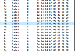
When we added a additional debug Variable, which was send out over CAN. unfortunately we can not reproduce the faulty behaviour with the debug variable.

Our ADC Channel:

Description ADC Channel ADC Port DMA CHANNEL Buffer Size Buffer Type
ADC_First1 18 A 3 100 uint16
ADC_First2 20 A 4 100 uint16
ADC_Additional1 4 A 1 30 uint16
ADC_Additional2 12 A 2 30 uint16

Configuration of the control Register: ADG2DMACR


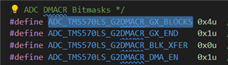
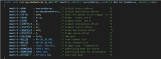
Here is our configuration and the function how the dma packet will be confugured.

________________________________________________

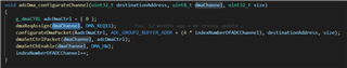
We have two questions:

1) what would be the effect of deactivation, while we validate the data and activate it afterwards again? Before we added the additional ADC Channel we deactivated the dma channel before we validated the data from the buffer.

Activation:
dmaREG
->HWCHENAS = (uint32)1U << channel;
Deactivation:
dmaREG->HWCHENAR = (uint32)1U << channel;

2) What is the effect of ADC_TMS570LS_G2DMACR_GX_BLOCKS ?
We had a Software which where ADC_TMS570LS_G2DMACR_GX_BLOCKS was  set to 2. In field tests it seams that this configuration was more stable, although we have 4 adc Channel which will be triggered by DMA.


Best Regards,

Thorben

  • Hi Thorben,

    TMS570LS_G2DMACR_GX_BLOCKS is not used if TMS570LS_G2DMACR_GX_BLK_XFER is not enabled. 

    Your configuration shows that the DMA request is generated for each write to ADC group2 memory. 

    Are 4 ADC channels triggered by the same trigger source? What are the buffers (size=100, and 30) used for?

  • Hey QJ,

    Thanks for your answer.

    As Trigger source we are using for all four Channel Frame Transfer.

    The buffer size is the length of the array for the destination. And is set to frameCount as well.

    e.G.
    uint16_t adc_first[100];
    adcDma_configurateChannel(destinationAddress = &adc_first[0], dmaChannel = 3, size = 100);

    Best Regards, Thorben

  • Got it. One trigger source is used for 4 channels: the ADC will start conversion for ADC channel 4, then channel 12, then channel 18, and then channel 20.

    In your ADC configuration, the BLK_XFER bit is not set, so the ADC module will generate the DMA request as soon as a conversion result gets written to the group’s results’ memory: the 1st DMA request is generated when the conversion result of ADC channel 4 is written to the group result memory, and the 2nd DMA request is generated when the conversion result of ADC channel 14 is written to the group result memory, etc. All the 4 DMA requests are from the same the DMA request 11. 

    How to guarantee DMA channel 1, channel 2, channel 3 and channel 4 are triggered in order of number?

    Can you enable BLK_XFER, so a DMA request is generated for 4 conversion results being available in the group’s results’ memory? 

    G2_BLOCKS = 4, and G1_BLK_XFER=1 --> ADC module will generate a DMA request at the end of 4th conversion. DMA controller should complete reading out 4 data before next set of 4 conversions complete.

  • Hey QJ,

    Thanks for your reply,

    Do we also modify the triggersource to block transfer?

    dmaCtrl->TType = Block_Transfer

    If we do so, the values in our buffer are mixed.

  • Do we also modify the triggersource to block transfer?

    No, please use the same trigger source for the ADC group2.

    The DMA request is only generated at the end of 4th conversion, you can keep using the FRAME_TRANSFER

  • The Element size should be changed to 4, and change the element destination offset to 4 too.

  • Thank for your, we will try it. Slight smile

    We have a result of our debug-Values and like to share it with you.

    The Issue came after 56h of testing. It looks a little bit confusing, however, i try to explain it:
    We have send the buffer values of ADC_First over CAN.
    On the left side, it looks like a curve of a capacity and some rectangles. Because we sending out many buffers, this is the behaviour which we have expected.

    From the middle to the right side all buffer values are almost equal. At that point we are sure that the values of the buffer has been switched.

    The values of ADC_First_1 looks like the Values of ADC_Additional_1.
    On a not Debug Message where we sending the average of the  ADC_Additional_1 buffer values, we have detected a small rectangle curve. Cause of this phenomen, we are sure that the values of the buffers has switched.

    ADC_First_1 <---> ADC_Additional_1.

    Best Regards,

    Thorben

  • We changed the configuration. When we increased the element size we got a mpu fault, so we kept it on 1.
    The buffer type and Read/Write Size is set to 32 bit.
    Now we can read the Channel-ID of the AD-Conversion and we send it out over CAN every 100ms.
    Byte 0 :  Channel 18;
    Byte 1 : Channel 20;
    Byte 2 : Channel 4;
    Byte 3 : Channel 12;

    For an undefined time the channel IDs are correct, however, in the Trace we see that after a while some of  them are incorrect.

    We don't have a clue why this behaviour happen. Our next try is to reinit the ADC-DMA module when, this behaviour starts. Let us know, if you got a better idea.


    Best Regards,

    Thorben

  • Hi Thorben,

    Do you enable the BLK_XFER bit? My suggestion is to use block transfer using one DMA channel. The DMA request is generated when the 4 conversion results is stored into the ADC memory. 

  • We have enablerd BLK_XFER. The good side, the results are not mixed anymore. However after a while there was no values into the buffer.

    We tried to enable Block Transfer Complete IRQ. For now it looks ok. longer tests are still running.

    What happens, if DMA_G2_END and G2_BLK_XFER is enabled ?

  • What happens, if DMA_G2_END and G2_BLK_XFER is enabled ?

    If G2_BLK_XFER and DMA _G2_END are enabled, the DMA data transfer starts when the last channel's conversion result is written to the result memory.

  • Thanks for your help

  • Dear TI-Support,

    we think we found the main reason:

    It appeared that the results were swapped, in fact the ADC result was invalid and the same ADC channel was triggered again. So the new value of the result was not in the expected ADC buffer and the DMA copied the invalid value to the application buffer. Our fifo size was 16, so if there were more than 4 results, the DMA engine didn't take the result into account.

    Thanks for your support