


Other Parts Discussed in Thread: MSP430F5529, MSP430G2553
Hello. I have encountered some problem using EK-TM4C123GXL ADC12. It seems like some of the settings is not quite clear for now.
I'll be delighted if any of the following problem is solved.
1. I'm using ADC sequence step configuration trying to control the adc sampling and interrupt.
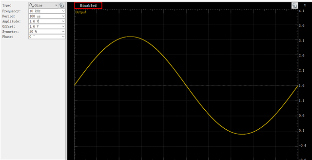
A 10kHZ sine signal is connected to PE3.
The Init settings is shown below and i'm quite sure that these peripherals are initialized in the main function in a proper order.(CLOCK->GPIO->ADC->Timer)
//////////////////////////////////////////////////////////////////////////////////////////////////////////CODE
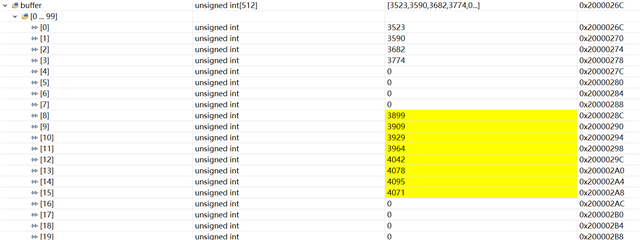
uint32_t buffer[512];
uint32_t i=0;
void Clock_Init()
{
SysCtlClockSet(SYSCTL_SYSDIV_2_5 | SYSCTL_USE_PLL | SYSCTL_OSC_MAIN |SYSCTL_XTAL_16MHZ); //80MHz system clock
}
void GPIO_Init()
{
SysCtlPeripheralEnable(SYSCTL_PERIPH_GPIOF);
while(!SysCtlPeripheralReady(SYSCTL_PERIPH_GPIOF));
GPIOPinTypeGPIOOutput(GPIO_PORTF_BASE,GPIO_PIN_1|GPIO_PIN_2);
}
void ADCHandler()
{
// uint32_t j,sum=0;
ADCIntClear(ADC0_BASE, 0);
ADCSequenceDataGet(ADC0_BASE, 0, buffer+8*i);
i++; //THE BREAKPOINT IS SET HERE
if(8*i>512-8) //Refill the data buffer
{
i=0;
}
}
void ADC_Init()
{
SysCtlPeripheralEnable(SYSCTL_PERIPH_ADC0);
//
// Enable the GPIO pin for ADC0 Channel 0 (PE3) which configures it for
// analog functionality.
//
SysCtlPeripheralEnable(SYSCTL_PERIPH_GPIOE);
GPIOPinTypeADC(GPIO_PORTE_BASE, GPIO_PIN_3);
ADCClockConfigSet(ADC0_BASE, ADC_CLOCK_SRC_PLL | ADC_CLOCK_RATE_FULL, 25); // 16MHz
//Using output of Timer0 to control the ADC sample time.
ADCSequenceConfigure(ADC0_BASE, 0, ADC_TRIGGER_TIMER, 0);
//ADC sequence step configuration
ADCSequenceStepConfigure(ADC0_BASE, 0, 0, ADC_CTL_CH0);
ADCSequenceStepConfigure(ADC0_BASE, 0, 1, ADC_CTL_CH0);
ADCSequenceStepConfigure(ADC0_BASE, 0, 2, ADC_CTL_CH0);
ADCSequenceStepConfigure(ADC0_BASE, 0, 3, ADC_CTL_CH0 | ADC_CTL_END |
ADC_CTL_IE);
//
// Since sample sequence 0 is now configured, it must be enabled.
//
ADCSequenceEnable(ADC0_BASE, 0);
//Register the adc interruput function and clear the interrupt flag
ADCIntRegister(ADC0_BASE,0,ADCHandler);
ADCIntClear(ADC0_BASE, 0);
// ADCSequenceDMAEnable(ADC0_BASE, 0);
ADCIntEnable(ADC0_BASE, 0);
IntEnable(INT_ADC0SS0);
}
void Timer_Init()
{
SysCtlPeripheralEnable(SYSCTL_PERIPH_TIMER0); //Enable Timer0
//Periodic count mode USING HALF WIDTH Timer_A (16bit)
TimerConfigure(TIMER0_BASE, TIMER_CFG_SPLIT_PAIR | TIMER_CFG_A_PERIODIC);
TimerLoadSet(TIMER0_BASE, TIMER_A, (SysCtlClockGet()/200000) - 1); // 200kHz sampling rate
//
// Enable the ADC trigger output for Timer A.
//
TimerControlTrigger(TIMER0_BASE, TIMER_A, true);
//
// Enable processor interrupts.
//
IntMasterEnable();
//
// Enable Timer 0 which will start the whole application process.
//
TimerEnable(TIMER0_BASE, TIMER_A);
}
/////////////////////////////////////////////////////////////////////////////////////////////////////////////////////
In my opinion i have have 4 new data when an interrupt occured.
When first interrupt occured:
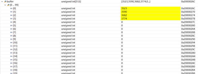
When second interrupt happend:
Does it mean that i should configure the ADC sequence step again in the interrupt handler?
Or there is something wrong in the initial setting?
I don't understand this situation since i just try to get 4 new data every time.
2.
Then i configure the step to meet the FIFO depth.
//////////////////////////////////////////////////////////////////////////CODE
//ADC sequence step configuration
ADCSequenceStepConfigure(ADC0_BASE, 0, 0, ADC_CTL_CH0);
ADCSequenceStepConfigure(ADC0_BASE, 0, 1, ADC_CTL_CH0);
ADCSequenceStepConfigure(ADC0_BASE, 0, 2, ADC_CTL_CH0);
ADCSequenceStepConfigure(ADC0_BASE, 0, 3, ADC_CTL_CH0);
ADCSequenceStepConfigure(ADC0_BASE, 0, 4, ADC_CTL_CH0);
ADCSequenceStepConfigure(ADC0_BASE, 0, 5, ADC_CTL_CH0);
ADCSequenceStepConfigure(ADC0_BASE, 0, 6, ADC_CTL_CH0);
ADCSequenceStepConfigure(ADC0_BASE, 0, 7, ADC_CTL_CH0 | ADC_CTL_END |
ADC_CTL_IE);
/////////////////////////////////////////////////////////////////////////////////////////
Some time later i stop the execution and using the Graph tool to watch the data acquired.

Since the sample rate is set to 200kHz and the input signal is a 10kHz sine wave, in my mind there should be 20 data point in one period.
But clearly there are more than 20 data points here in on period.( and also less than 8*20=160 data points)
Then the sample rate is changed to 100kHz:
TimerLoadSet(TIMER0_BASE, TIMER_A, (SysCtlClockGet()/100000) - 1);
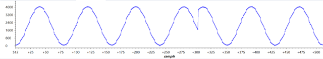
Then 50kHz:
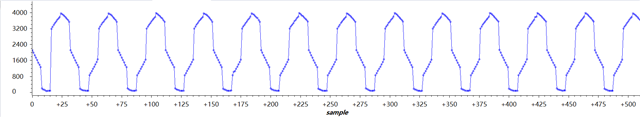
I think the 50kHz sampling rate will not be large enough to rebuild the sine wave(despite that fs>2fm)
Does it mean that i should get the average value of every 8 new data in the interrupt function and can't treat the 8 new data in the buffer as a sequence of sampling results under the set sampling rate?
OR maybe i just need to use Sequence 3 and get one new data every time?
Will we get the same result under these two different settings?
I HAVE DO SOME WORK ON MSP430F5529 AND MSP430G2553. The timer (output mode)can control the sampling well by using repeat single sampling mode. And sure i will get the expected data under the expected sample rate.
Now I managed to do the same work on this device and it seems like there is a big difference on the ADC settings. As stated above, I have problem understanding the process of the adc function.
I will be soooooo grateful if i can fully understand the adc data i got.
Best regards

