This thread has been locked.

If you have a related question, please click the "Ask a related question" button in the top right corner. The newly created question will be automatically linked to this question.

TM4C123GH6PM: ADC0 Sampling with uDMA killed a TIMTER PWM Signal

Part Number: TM4C123GH6PM
Other Parts Discussed in Thread: EK-TM4C1294XL

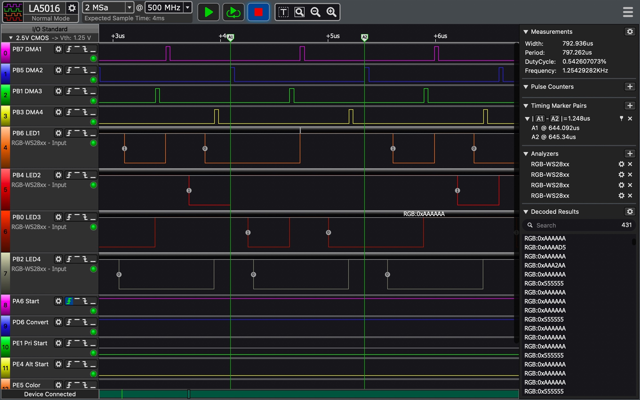
I use 4 Timers as PWM Mode.

Every Timer has his own DMA Interrupt Signal to transfer 1 Item from Memory to his own Match Register to Change the DutyCycle.

This is running good. But when I am activate uDMA for ADC Sampling to memory. My Timers PWM Signal sometimes is not running for one PWM Period.

Why? I test it so much to find the error. Iam out of ideas.

Here is a Picture. The failure is on channel 5 PB4 LED2. The Periode is complete high. When the uDMA signal comes to late, in the match register is an older value.

It is helpfuly to poste the code? That has more than 3000 lines code.

  • Hi,

      I'm not really sure what is the problem. I've not see a problem reported as such. Can you answer a few questions so I have better clarify to your application?

      - How many uDMA channels are you using in your entire application? 

      - What are PB7, PB5, PB1 and PB3 on your capture? How are these signal generated? You denote them as PB7 DMA and so on. Are these signals generated by using uDMA too?

      - Which uDMA channels are you using? You can also answer by which Timer modules you are using. 

      - What are the priorities among the uDMA channels? By default, the lower the channel index the higher priority. Therefore, ADC SS0 will have lower priority than Timer 3 but higher than Timer 0. But you can also set a channel to high priority. See below description.

    9.2.2 Priority
    The uDMA controller assigns priority to each channel based on the channel number and the priority
    level bit for the channel. Channel number 0 has the highest priority and as the channel number
    increases, the priority of a channel decreases. Each channel has a priority level bit to provide two
    levels of priority: default priority and high priority. If the priority level bit is set, then that channel has
    higher priority than all other channels at default priority. If multiple channels are set for high priority,
    then the channel number is used to determine relative priority among all the high priority channels

      - For PB4 LED2, can you set it to higher priority while setting other channels to lower (which is the default) priority? Will you see any different behavior? I want to know if priority makes a difference?

      - For experiment purpose, can you set the period of each PWM to a wider period or at least for PB4 LED2? I wonder if uDMA has enough time to write to the match register before the end of the period? 

      - For experiment purpose, can you replace PB4 ( I suppose you use T1CCP0 for PB4) by another timer? For example, replace T1CCP0 by T4CCP0 on PC0? Right now you are using all the PortB pins. Just curious if the failure pin is moved out of PortB to another pin like PortC0. 

  • Thank you for your quick feedback.

    I have the same problem sporadically with all 4 timers.

    But only if I record at the same time also with the ADC0 via uDMA.

    I have already tried to play with the priorities, but without success.

    I use the TIMER PWM Output from a GPIO and make wire bridge to another GPIO for the uDMA request.

    So it is possible to transfer one item per uDMA request. because the GPIO ports are able to use singe requests. These Signals are for the uDMA Request.

    EDIT:

    Sorry I did not answer all your questions.

    I use 4 uDMA CHannels for the PWM Signals and 1 Channel for Sampling Data from ADC via uDMA to Memory.

    PB7, PB5, PB1 and PB3 these signals are created by timers. 

    // Need to be bridged: PB7 <---> PA7

    // Need to be bridged: PB5 <---> PC7

    // Need to be bridged: PB1 <---> PD3

    // Need to be bridged: PB3 <---> PF2

    // Timer 0A is the data signal 1: PB6

    // Timer 0B is the udma trigger signal to GPIO: PB7

    // Timer 1A is the data signal 2: PB4

    // Timer 1B is the udma trigger signal to GPIO: PB5

    // Timer 2A is the data signal 3: PB0

    // Timer 2B is the udma trigger signal to GPIO: PB1

    // Timer 3A is the data signal 4: PB2

    // Timer 3B is the udma trigger signal to GPIO: PB3

    I use the uDMA Channel: 4,6,7,17 for the Signal and Channel 14 for the ADC0

    Code:

    void uDMAGPIOAIntHandler(void)
    {
        //
        // 1 uDMA Channel = 16 Bytes
        // Byte 0 - 3 = Source End Pointer
        // Byte 4 - 7 = Destination End Pointer
        // Byte 8 - B = Control Word <--- We need this adress offset
        // Byte C - F = Unused
        //
        // uDMA Channel 4 Primary = 4 * 16 + 8 = 72
        // uDMA Channel 4 Alternate = (32 + 4) * 16 + 8 = 584
        //
        
        if (uDMAControlTable[72] == 0 && uDMAControlTable[584] == 0)
        {
            // ------------------------------------------------------------
            //
            // Timer 0A counter value
            //
                // TIMER0_BASE = 0x40030000
                // TIMER_O_TAV = 0x00000050
                //             = 0x40030050
            // (*((volatile uint32_t *)0x40030050))
            //
            // ------------------------------------------------------------
            while ((*((volatile uint32_t *)0x40030050)) > SIGNAL_1)
            {
                // ...waiting the signal is 0
            }
            
            // ------------------------------------------------------------
            //
            //MAP_TimerDisable(TIMER0_BASE, TIMER_BOTH);
            //
                // TIMER0_BASE = 0x40030000
                //
                // TIMER_O_CTL = 0x0000000C
                // 
                // TIMER_CTL_TAEN = 0x00000001
                // TIMER_CTL_TBEN = 0x00000100
            (*((volatile uint32_t *)0x4003000C)) &= ~0x00000101;
            // 
            // ------------------------------------------------------------
            
            // ------------------------------------------------------------
            //
            // Timer counter value reset
            //
                // TIMER0_BASE = 0x40030000
            
                // TIMER_O_TAV = 0x00000050
                // TIMER_O_TBV = 0x00000054
            (*((volatile uint32_t *)0x40030050)) = 0x00000000;
            (*((volatile uint32_t *)0x40030054)) = 0x00000000;
            //
            // ------------------------------------------------------------
        }
        
        if (uDMAControlTable[72] == 0)
        {
            DEBUG_PE2 = GPIO_PIN_2; // DMA Pri
        }
        if (uDMAControlTable[584] == 0)
        {
            DEBUG_PE3 = GPIO_PIN_3; // DMA Alt
        }
        
        DEBUG_PE2 = 0; // DMA Pri
        DEBUG_PE3 = 0; // DMA Alt
        uDMADoneCounter = tick10ms;
    }

  • Hi,

      You have over 3000 lines of code and I really have hard time following after hours of reading. This is what I understand so far based PB7 -> PA7 -> PB6.

      1. You use Timer0_B to generate a PWM on PB7.

      2. The PB7 is connected to PA7 configured as an GPIO input.

      3. PA7 will trigger a uDMA transfer on channel 4.

      4. uDMA channel 4 is configured to transfer from memory to the match register of Timer0_A which is configured for PWM on PB6 pin.

      I really don't understand why you need to connect PB7 to PA7 for a uDMA trigger using GPIO. Why don't you consider to configure Timer0_B for periodic timeout and let the timeout directly trigger uDMA on channel19. Use channel 19 to change the duty cycle of timer0_A for PB6. 

      I also don't understand about the ISR such as uDMAGPIOAIntHandler. Why are they needed? If PA7 is used as uDMA request, it should not even generate an interrupt, correct? Under what circumstances will PA7 not generate uDMA request and generate interrupt instead. In the ISR, I see you manipulate the uDMA control table manually on their fields. I have not seen anyone doing this. I feel it is quite risky. How can you guarantee the control information is not used by the uDMA kernel in the middle while you are writing to them in the ISR. The control table is meant to be initialized in the beginning of uDMA setup. Why do you need to manipulate the table anyway and what are trying to change?

     I have also three comments on your ADC setup.

      1. Why do you want to use ADC_TRIGGER_ALWAYS? I will suggest you use a timer trigger or processor trigger with better control especially for a complex application like you have. 

      2. Why do you have ADC_CTL_IE twice in your code for step 3 and step 7. You are trying to generate two uDMA requests per sequencer? Why? You should remove the ADC_CTL_IE for step 3. 

      3. You didn't specify which step is the last step in the sequencer. This will not work. Please refer to ADC example in TivaWare. You need to have a ADC_CTL_END flag for step 7. 

    MAP_ADCSequenceConfigure(ADC0_BASE, 0, ADC_TRIGGER_ALWAYS, 0);
    MAP_ADCSequenceStepConfigure(ADC0_BASE, 0, 0, ADC_CTL_CH5);
    MAP_ADCSequenceStepConfigure(ADC0_BASE, 0, 1, ADC_CTL_CH5);
    MAP_ADCSequenceStepConfigure(ADC0_BASE, 0, 2, ADC_CTL_CH5);
    MAP_ADCSequenceStepConfigure(ADC0_BASE, 0, 3, ADC_CTL_CH5 | ADC_CTL_IE);
    MAP_ADCSequenceStepConfigure(ADC0_BASE, 0, 4, ADC_CTL_CH5);
    MAP_ADCSequenceStepConfigure(ADC0_BASE, 0, 5, ADC_CTL_CH5);
    MAP_ADCSequenceStepConfigure(ADC0_BASE, 0, 6, ADC_CTL_CH5);
    MAP_ADCSequenceStepConfigure(ADC0_BASE, 0, 7, ADC_CTL_CH5 | ADC_CTL_IE);

  •  1. You use Timer0_B to generate a PWM on PB7.
    
      2. The PB7 is connected to PA7 configured as an GPIO input.
    
      3. PA7 will trigger a uDMA transfer on channel 4.
    
      4. uDMA channel 4 is configured to transfer from memory to the match register of Timer0_A which is configured for PWM on PB6 pin.

    Right.

    I really don't understand why you need to connect PB7 to PA7 for a uDMA trigger using GPIO. Why don't you consider to configure Timer0_B for periodic timeout and let the timeout directly trigger uDMA on channel19. Use channel 19 to change the duty cycle of timer0_A for PB6. 

    I also tried this first with a timer directly with uDMA. But I could not configure the uDMA to send only one item per request. In the documentation on page 589 it says in the table that the GP timers do not create a single request event. So I had to think about something. And I came to the idea to use a GPIO as uDMA single request.

    I also don't understand about the ISR such as uDMAGPIOAIntHandler. Why are they needed? If PA7 is used as uDMA request, it should not even generate an interrupt, correct? Under what circumstances will PA7 not generate uDMA request and generate interrupt instead. In the ISR, I see you manipulate the uDMA control table manually on their fields. I have not seen anyone doing this. I feel it is quite risky. How can you guarantee the control information is not used by the uDMA kernel in the middle while you are writing to them in the ISR. The control table is meant to be initialized in the beginning of uDMA setup. Why do you need to manipulate the table anyway and what are trying to change?

    I need the ISR uDMAGPIOAIntHandler to switch off the signal. As soon as the uDMA Primary and Alternate Transfer are finished, I turn off the timer.
    Because this has to be done very fast, I decided to work without TivaWare Lib in this part of the code.
    But I don't change the uDMA structure. I check for 2 states in the uDMA structure. And turn off the timer.

    1. Why do you want to use ADC_TRIGGER_ALWAYS? I will suggest you use a timer trigger or processor trigger with better control especially for a complex application like you have. 

    Thanks for the tip. It was also planned to control the ADC with a timer in the future. With the current config of the ADC I have a sampling rate of 31250 Hertz.
    Because I want to record music I need one of 44.100 Hz. But for now the 31250 Hertz is enough for me.
    The Trigger Always only means that the ADC records with its set clock or ?

     2. Why do you have ADC_CTL_IE twice in your code for step 3 and step 7. You are trying to generate two uDMA requests per sequencer? Why? You should remove the ADC_CTL_IE for step 3. 

    I did it this way because that is what I understood. If I want to record continuously over a longer period of time. Here now 1024 samples. Then I have to configure it like this. I understood that Sample Sequencer should always be emptied with 50% so that the other 50% can be filled again. 

    EDIT:

    I have tested this. Now my recording takes twice as much time. Before the recording needed 32,6ms. Why is this so ?

    The problem is not gone.

    3. You didn't specify which step is the last step in the sequencer. This will not work. Please refer to ADC example in TivaWare. You need to have a ADC_CTL_END flag for step 7. 

    Here I'm unsure now, but I'll look again in older versions of my code.

    EDIT: I use it. And the problem is not gone.

  • Hi,

      My understanding is that without the uDMA to ADC, the 8 PWMs (4 of them are used as a trigger for uDMA request and the other 4 are the real PWM with variable duty cycle) are working correctly. Please confirm again if this the case. 

      Can you provide some data points? 

      - With only uDMA for ADC operating and all other uDMA channels for timers are disabled, will uDMA for ADC transfer work successfully? What I want to know is that your uDMA setup for ADC is correct. If it is working and we already know the fact that the 8 PWM are working correctly without the ADC, then it means the software side is most likely not a problem. If it is truly not a software issue then I feel it is more a performance issue where TM4C123 may have reached some performance bottleneck. Note it is not just uDMA transfers but also all the data post processing the CPU within the timeframe (44kHz) is needed to perform that may have reached some performance bottleneck. 

      - What will happen if you start with fewer number of PWM? Please try only one uDMA channel where timer0_B PWM on PB7 -> PA7 -> uDMA channel 4 -> timer0_A PWM on PB6. Will you see problem with only two uDMA channels - channel 4 and channel  14?

      - Gradually increase the total number of uDMA channels from 2 to 3. This time you will also enable for uDMA channel 5. This means you have channel 4, 5 and 14 operating at the same time. Will you see problem with 3 channels?

      - You can go on to increase another channel. When will you start to see problem? What I want you to confirm is that as more channels are introduced, the more apparent the problem will be. On the contrary, no problem is observed with few channels. If you say that you will always see problem no matter the number of channels then need to go back to the software side. 

      - You not only use ADC0 but also ADC1? Will disabling ADC1 make a difference?

      - Do you have a TM4C129 LaunchPad? TM4C129 is a higher performance processor than TM4C123. I'm curious to know if TM4C129 has the same issue. If TM4C129 can run the same code without the reported issue then it is clear that it is a performance issue. 

      - I understand 44kHz is the ideal sampling frequency for audio application.  Have you tried 22kHz or lower as an experiment? Will you see the same problem? Again, I'm trying to determine if some sort of performance bottleneck is reached. 

  • Thanks again for trying to help me.
    I have no idea where the error is. Software or hardware and am already a bit desperate.
    I spent the whole day again today with it. To narrow down my error further. I have also already actually instead of 4 LED signals only with 1 LED signal times to work. But still the same error picture.
    I can say now, however, that if I go back to an older software version. Then it goes. But in this older software version I can only create 1 LED signal. But I can create 1 LED signal and sample with uDMA and ADC0 at the same time.
    Without error. This smells like it could be a software error. Because old software version with 1 LED signal and uDMA with ADC0 sampling works but new software version with 1 LED and uDMA does not work.
    The software configuration is different.

    void GPIOPortBIntHandler(void)
    {
        MAP_GPIOIntClear(GPIO_PORTB_BASE, GPIO_INT_DMA);
        uDMADoneCounter = tick10ms;
        
        DEBUG_PE1 = GPIO_PIN_1; // DMA INT
        
        if ((uDMAChannelModeGet(UDMA_CH5_GPIOB | UDMA_PRI_SELECT) ==
                                UDMA_MODE_STOP))
        {
            DEBUG_PE3 = GPIO_PIN_3; // PRI STOPPED
        }
        if ((uDMAChannelModeGet(UDMA_CH5_GPIOB | UDMA_ALT_SELECT) ==
                                     UDMA_MODE_STOP))
        {
            DEBUG_PE4 = GPIO_PIN_4; // ALT STOPPED
        }
        
        DEBUG_PE1 = 0; // DMA INT
        DEBUG_PE3 = 0; // PRI STOPPED
        DEBUG_PE4 = 0; // ALT STOPPED
    }

    This is a little different.

    I only use TIMER1 and PB4 is the LED data signal. And PB0 is connected with PB5 with a cable. For the uDMA request.

    Here I do not switch off the LED signal yet either. The LED chip does not see a signal at 1-2% DutyCycle.

    These were my new findings.

    My understanding is that without the uDMA to ADC, the 8 PWMs (4 of them are used as a trigger for uDMA request and the other 4 are the real PWM with variable duty cycle) are working correctly. Please confirm again if this the case. 

    Yes it is right. I make the recording and wait until it is ready. Then I send the LED data.

     Can you provide some data points? 

    You mean the record data from the ADC0 ? It comes from a microphone.

    With only uDMA for ADC operating and all other uDMA channels for timers are disabled, will uDMA for ADC transfer work successfully?

    yes.

    What I want to know is that your uDMA setup for ADC is correct. If it is working and we already know the fact that the 8 PWM are working correctly without the ADC, then it means the software side is most likely not a problem. If it is truly not a software issue then I feel it is more a performance issue where TM4C123 may have reached some performance bottleneck. Note it is not just uDMA transfers but also all the data post processing the CPU within the timeframe (44kHz) is needed to perform that may have reached some performance bottleneck. 

    That's what I thought too, but as described above. If I take an older software version. Can I sample with 1 LED data signal simultaneously with ADC0. With my newer software with 4 LED data signals it does not work even if I have only 1 LED signal activated.

    What will happen if you start with fewer number of PWM? Please try only one uDMA channel where timer0_B PWM on PB7 -> PA7 -> uDMA channel 4 -> timer0_A PWM on PB6. Will you see problem with only two uDMA channels - channel 4 and channel  14?

    have already tried this today. But has brought no success.

    Gradually increase the total number of uDMA channels from 2 to 3. This time you will also enable for uDMA channel 5. This means you have channel 4, 5 and 14 operating at the same time. Will you see problem with 3 channels?

    I have not done now, because 1 signal already does not work.

    You can go on to increase another channel. When will you start to see problem? What I want you to confirm is that as more channels are introduced, the more apparent the problem will be. On the contrary, no problem is observed with few channels. If you say that you will always see problem no matter the number of channels then need to go back to the software side. 

    I had also thought this. But even with one channel it does not work.

    You not only use ADC0 but also ADC1? Will disabling ADC1 make a difference?

    So I have always used the ADC0 even with the older software version. The ADC1 is now new in the code. But it is currently not used. It is only prepared for the future. Possibly to evaluate 2 microphones.

    Do you have a TM4C129 LaunchPad? TM4C129 is a higher performance processor than TM4C123. I'm curious to know if TM4C129 has the same issue. If TM4C129 can run the same code without the reported issue then it is clear that it is a performance issue. 

    Sorry no.

    EDIT:

    I have just looked in the documentation of the EK-TM4C1294XL. On page 682 it says in the table that no single request is possible. Neither via a GPIO nor via a timer.

    I understand 44kHz is the ideal sampling frequency for audio application.  Have you tried 22kHz or lower as an experiment? Will you see the same problem? Again, I'm trying to determine if some sort of performance bottleneck is reached. 

    No. I can try this tomorrow.

  • I can say now, however, that if I go back to an older software version. Then it goes. But in this older software version I can only create 1 LED signal. But I can create 1 LED signal and sample with uDMA and ADC0 at the same time.

    If the older version works with 1 LED signal and ADC at the same time, I will suggest you go back to the older version and confirm one more time that it is still working. After you confirm it is working as expected then you will add channel at a time for 2 LEDs and then 3 LEDS and so forth. I think this will be the safest approach. It will be much easier for you to debug along the way when you start with something simple and working and then gradually increase the number of channels. 

  •  I also don't understand about the ISR such as uDMAGPIOAIntHandler. Why are they needed? If PA7 is used as uDMA request, it should not even generate an interrupt, correct? Under what circumstances will PA7 not generate uDMA request and generate interrupt instead. In the ISR, I see you manipulate the uDMA control table manually on their fields. I have not seen anyone doing this. I feel it is quite risky. How can you guarantee the control information is not used by the uDMA kernel in the middle while you are writing to them in the ISR. The control table is meant to be initialized in the beginning of uDMA setup. Why do you need to manipulate the table anyway and what are trying to change?

    I hadn't understood exactly what you meant by that. And I thought that because I only read, it's not a problem.

    When I removed these direct queries. The problem was also gone.

    I mean these lines: if (uDMAControlTable[72] == 0 && uDMAControlTable[584] == 0) ....

      I really don't understand why you need to connect PB7 to PA7 for a uDMA trigger using GPIO. Why don't you consider to configure Timer0_B for periodic timeout and let the timeout directly trigger uDMA on channel19. Use channel 19 to change the duty cycle of timer0_A for PB6.

    Is this possible?
    But I want to send only one item per uDMA request.
    I tried this once, but did not succeed.

  • I mean these lines: if (uDMAControlTable[72] == 0 && uDMAControlTable[584] == 0) ....

    I'm not too sure why are you checking for the entire primary and alternate control word (the entire 32 bit) to be zero? The control word has many control fields and why do you need all of them to zeros?

    When I removed these direct queries. The problem was also gone.

    Glad that this resolves your issue. 

    But I want to send only one item per uDMA request.
    I tried this once, but did not succeed.

    Looks like timer module only generates burst request. Per datasheet, if you configure the arbitration size to 1 then it should only transfer one item even though it is a burst type. However, this may not work for you. The reason is that after one item is transferred out and if there are no more higher priority channels to be served, it will try to transfer the remaining items. You might need to set the number of items to one as well. You will need to determine if your application can be adapted to this limitation. Otherwise, you need to use what you currently do - route the PWM to an GPIO input and use GPIO to generate single request. 

    Burst Request
    When a burst request is detected, the μDMA controller transfers the number of items that is the
    lesser of the arbitration size or the number of items remaining in the transfer. Therefore, the arbitration
    size should be the same as the number of data items that the peripheral can accommodate when
    making a burst request. For example, the UART generates a burst request based on the FIFO trigger
    level. In this case, the arbitration size should be set to the amount of data that the FIFO can transfer
    when the trigger level is reached. A burst transfer runs to completion once it is started, and cannot
    be interrupted, even by a higher priority channel. Burst transfers complete in a shorter time than the
    same number of non-burst transfers.

  • thanks for you help!

    Can you confirm that no read access to the udma control table is allowed? except via the driver library.

    I'm not too sure why are you checking for the entire primary and alternate control word (the entire 32 bit) to be zero? The control word has many control fields and why do you need all of them to zeros?

    i would like to use this command to see if the transfer is ready.

  • Can you confirm that no read access to the udma control table is allowed? except via the driver library.

    I don't see any reason why the control table cannot be just read by your custom code. Writing to the control table while in the middle of a transfer may cause problem but that is not what you are doing. 

  • Sorry, but the error is not gone.
    I have as you have written. I reduced the LED signals from 4 to 3, then to 2 and then to 1. I could not fix the error by doing this.
    The error with the timer comes only, if I send at the same time with the ADC0 music sample and then at the same time with the timer the Led signal.
    As soon as I send only the LED signal without sampling music with the ADC0, the timer runs.

    I have 2 problems with the timer.
    That one period disappears completely. Like on the picture above. (PB4 LED 2).
    Or the uDMA does not manage to update the match register in time.

    What can cause a timer period failure?

    If I use a LED signal i.e. Timer1A and Timer1B and at the same time with the ADC0 sample. Can this be a performance problem ?

  • I thought you wrote below at one point of time your older version of code was working for one LED with uDMA+ADC0. 

    "I can say now, however, that if I go back to an older software version. Then it goes. But in this older software version I can only create 1 LED signal. But I can create 1 LED signal and sample with uDMA and ADC0 at the same time."