This thread has been locked.

If you have a related question, please click the "Ask a related question" button in the top right corner. The newly created question will be automatically linked to this question.

TMS570LC4357-EP: DMA Bus Error on first 16 transfer from L2SRAM to SPI2.TX

Part Number: TMS570LC4357-EP
Other Parts Discussed in Thread: HALCOGEN

L2SRAM is MPU mapped in user mode.  DMA already working OK from L2SRAM to SCI4.TX 

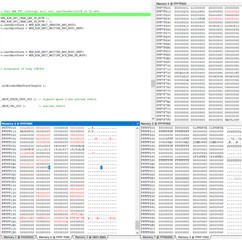
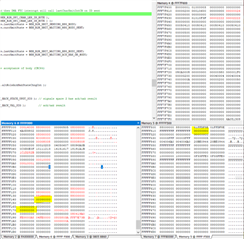
On a 16 bit transfer, I get DMA Bus Error (at ESM) on very first transfer from address 0x08058868 (L2SRAM) to 0xFFF7F63E (SPI2.TXDATA)

The application uses the SPI in legacy mode (so DMA channel 3). Only enabling SPI2CLK and SPI2SIMO pins as functional ones.

Manual sending of a single word (done before in the code, works fine and confirmed on scope.) First DMA access, that fails, creates no output at SPI SIMO.

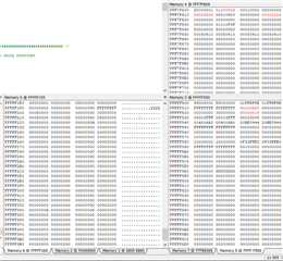
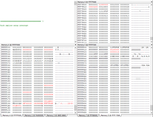
The SDC only reports 0 on all of its registers. So I have no clue on cause of DMA Bus Error.

  • To make it clear.  I do not enable the RX pin and don't plan to use it.  I am not configuring any RX DMA.  The link is unidirectional because only enabling SPI2CLK and SPI2SIMO.

    Manually (non-DMA) sending works fine.  Setting DMAREQEN and then SPIEN does initiate a transfer but the access gives DMA Bus Error (at ESM).  Source address is OK and destination address is OK for a 16 bit transfer.

  • More details:

    No DMA working packet generated at DMA Bus Error.

    Channel 3 Control Packet Content:

    0x08058868 0xFFF7F63E 0x001C0001 0x00000000 0x00005008 0x00000000 0x00000000

    So addresses are OK content and alignment-wise.

    16 bits source & destination Frame transfer of 28 times 1 element per DMA req.

    post-incr of source addr

    fix dst addr

    Any idea of DMA Bus Error cause in this context? (Again SDC shows all 0x00000000)

  • Hi, 

      You said SCI4 works. Which channel do you use for SCI4? Can you show the control packet for SCI4? For experiment, what if you use DMA channel 3 for SCI4, will SCI4 still work? 

      Can you also show the dump of DMA registers when you see the bus error?

  • SCI4.TX is more tricky since the source is DMAREQ[43], so I had to assign it to channel 31 that I wasn't using.

    About the DMA registers, there too many of them, you will need to be more specific.  

    By staying in same thread, I kept the default channel 3 assignment to DMAREQ[3] which is SPI2.TX in legacy. SPNS195C p. 124

  • Hi,

     I assume you are seeing ESM GP1.11, correct?

      Can you CCS register window to show the BERFLAG register in the DMA module?

      How many DMA channels have you set up? Is it only channel 3 or several channels?

  • I highlight in yellow for BERFLAG at 0xFFFFF144, BEROFFSET at 0xFFFFF170 and both show 0. The ESMSR1 at 0xFFFFF519 is also 0. There is no DMA bus error as far as I can see unless you clear these flags in software. For experiment, Will you get bus error if you use SPI1 or other SPI3/4/5? 

  • Sorry DMA Bus Error is G1.20

    SCI4.TX is active.  Also DMA between memory and CRC2 register in lower priority.  Also other peripherals are set in hi priority.

  • No BERFLAG because always 0 on this device.  TRM p. 751, section 20.3.1.42

  • Ok. I see the same note too. But your ESM is all zero to me. GP1.20 is not set in your memory window. 

  • Sorry. The  last one was just before the error.  Here is the new one.

  • Here with Ozone-flagged register just after DMA Bus Error. 


  • Have to go. Let's continue tomorrow morning.  Thanks for your response Charles.

  • Hi,

      As suggested before, for experiment to isolate problem, can you simplify your code to only have one DMA channel working on SPI2 and no other channels? Can you repeat the same problem on other SPI, e.g. SPI1, SPI3? Looking at your below control packet I cannot see a problem. 

    0x08058868 0xFFF7F63E 0x001C0001 0x00000000 0x00005008 0x00000000 0x00000000

  • Hi Charles.  Thanks for confirming the config. is OK. 

    I have disable the other DMA based activities and the problem remains.

    chanl_cp->dev_p->GCR1.reg.SPIEN = 0U;
    chanl_cp->dev_p->INT0.reg.DMAREQEN = 1U; // Enable DMA req at MibSPI level
    chanl_cp->dev_p->GCR1.reg.SPIEN = 1U;

    Any chance the previous code snippet isn't the right enabling sequence, where the SPI wouldn't be actually ready fast enough to respond to the DMA request because the SPI enabling wouldn't be fast enough?

  • Do you happen to know why the SDC registers read 0x0000000 instead of giving more info on the cause of the DMA Bus Error?

  • I have change the order of initialization:

    disabling DMA, setting of control packet, enable SPI DMAREQ, enabling SPIEN, Enable channel 3 DMA HARD REQ, then enable DMA.

    And I get same results.  So I think, SPI and DMA are working fine and probably should focus on something purely related to the read from memory or the right to SPI.TXDATA actions.

  • Hi,

      Have you tried the HalCoGen MibSPI DMA example? If not, can you please try as is first and later adapt to your needs? 

  • I do not have this code on hand and the platform I am working on is OEM.  Could you email me the .zip of the example and I will study it and see how easy I can insert it in my code as test-code.  Thanks.

  • Please give response to SDC related question.

  • Do you happen to know why the SDC registers read 0x0000000 instead of giving more info on the cause of the DMA Bus Error?

    SDC contains the control/status registers pertaining to the CPU Interconnect. If it reads zero then there is no error reading from L2RAM. The DMA as you configure is for PortA Read and PortB write. DMA portA is an initiator on the CPU Interconnect while DMA portB is an initiator connected to Peripheral Interconnect where SCI4/SPI2 are the slaves. The data flow would be to read L2RAM using DMA portA and write to slaves on Peripheral Interconnect using DMA PortB. The bus error must be generated from the Peripheral Interconnect side because bus error is normally generated by the slaves or the Peripheral Interconnect due to illegal address or illegal access. Did you enable the peripherals? Normally, if you use the standard startup the periphInit() would have been called to initialize the peripherals. Can you check if you enable all the peripherals?

    void periphInit(void)
    {
    
    /* USER CODE BEGIN (9) */
    /* USER CODE END */
    
        /** - Disable Peripherals before peripheral powerup*/
        systemREG1->CLKCNTL &= 0xFFFFFEFFU;
    
        /** - Release peripherals from reset and enable clocks to all peripherals */
        /** - Power-up all peripherals */
        pcrREG1->PSPWRDWNCLR0 = 0xFFFFFFFFU;
        pcrREG1->PSPWRDWNCLR1 = 0xFFFFFFFFU;
        pcrREG1->PSPWRDWNCLR2 = 0xFFFFFFFFU;
        pcrREG1->PSPWRDWNCLR3 = 0xFFFFFFFFU;
    
        pcrREG2->PSPWRDWNCLR0 = 0xFFFFFFFFU;
        pcrREG2->PSPWRDWNCLR1 = 0xFFFFFFFFU;
        pcrREG2->PSPWRDWNCLR2 = 0xFFFFFFFFU;
        pcrREG2->PSPWRDWNCLR3 = 0xFFFFFFFFU;
    
        pcrREG3->PSPWRDWNCLR0 = 0xFFFFFFFFU;
        pcrREG3->PSPWRDWNCLR1 = 0xFFFFFFFFU;
        pcrREG3->PSPWRDWNCLR2 = 0xFFFFFFFFU;
        pcrREG3->PSPWRDWNCLR3 = 0xFFFFFFFFU;
    
        /** - Enable Peripherals */
        systemREG1->CLKCNTL |= 0x00000100U;
    
    /* USER CODE BEGIN (10) */
    /* USER CODE END */
    
    }

  • Thanks for the clue,  My power settings were OK.  But the protection wasn't updated.  So SCI4 allowed user-mode write but not SPI2.  So now it is working since DMA is working user-mode accesses.