This thread has been locked.

If you have a related question, please click the "Ask a related question" button in the top right corner. The newly created question will be automatically linked to this question.

TMS570LC4357: Fapi_Error_OtpChecksumMismatch error during Flash driver initialization

Part Number: TMS570LC4357
Other Parts Discussed in Thread: HALCOGEN, TMS570LS3137

Hi Team,

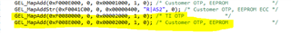
I am using the Flash library F021 from https://www.ti.com/tool/HERCULES-F021FLASHAPI for TMS570LC4357 HDK.

During initialization of Flash library the function Fapi_initializeFlashBanks() returns Fapi_Error_OtpChecksumMismatch. 

I am using F021_API_CortexR4_BE.lib.

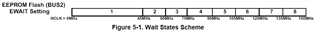
Fapi_initializeFlashBanks() is called with 160MHz. The system clock is also set to 160MHz.

If F021_API_CortexR4_BE_L2FMC.lib or F021_API_CortexR4_BE_L2FMC_V3D16 is used, the call to function Fapi_initializeFlashBanks() hangs.

Could you kindly guide to solve the issue?

  • Hi Divya,

    For TMS570LC4357 device, the "F021_API_CortexR4_BE_L2FMC.lib" should be used. The system clock (for example 150MHz) should be used by "Fapi_initializeFlashBanks()".

  • Hi Wang, 

    Whether the system clock and the flash driver clock must be same value?

    In my case I use 160MHz as system clock and also pass 160MHz to the function Fapi_initializeFlashBanks(). Is this correct?

  • If F021_API_CortexR4_BE_L2FMC.lib is used, there is no return value from the function Fapi_initializeFlashBanks() and it hangs.

  • The Flash read control register FRDCNTL is initialized as described in the related post. The RWAIT and EWAIT bits are set. But still I face the same issue.

  • The system clock is HCLK. Is the PLL or GCLK 160MHz too in your configuration? 

  • The maximum HCLK or system clock for TMS570LC43x is 150MHz. Can you try 80MHz system clock for Fapi_initializeFlashBanks()?

  • I tried with 150MHz and its same behavior. 

    One question : In the TMS570LC4357 HDK, the LED D1 nError is always RED. Could you kindly guide regarding this?

  • not always. Please refer to the errata Device#56:

    DEVICE#56 nERROR assertion on debugger connect

    Severity 4-Low

    Expected Behavior No errors should be detected when connecting to the device by JTAG Issue Sometimes a CPU compare error (ESM Group 2 channel 2) is generated when the debugger connects to device.

    Condition Upon a debugger initially connecting to the device.

    Implication(s) The nError pin will toggle upon initial connection with the debugger.


    Workaround(s) Clear the nERROR by writing 0x5 to the ESMEKR key register in the ESM module and ignore the nERROR pin toggle which happens immediately upon the debugger connecting.

  • Could we kindly set up debug session to find out why the return value is Fapi_Error_OtpChecksumMismatch?

  • Hi Divya,

    Can you share your two halcogen configuration files with me: *.hcg and *.dil?

    Please refer to the example code of sing F021 Flash API in TMS570LC43x bootloader:

    https://git.ti.com/cgit/hercules_examples/hercules_examples/tree/Bootloaders?h=master

  • Could you please say where to look for Errata description? i could not find in the datasheet.

    I am not using HALcogen, instead manually setting the registers.

    Can I use the sys_startup files from your provided path https://git.ti.com/cgit/hercules_examples/hercules_examples/tree/Bootloaders/SafetyMCU_Bootloaders/HALCoGen/TMS570LC43x to adapt to my startup directly or do I have to do any more modifications?

  • I found the Silicon Errata doku www.ti.com/.../spnz180d.pdf

  • Can I use the sys_startup files from your provided

    Yes, you can. 

    Have you configured the flash wait states properly?

    flashWREG->FRDCNTL = 0x00000000U | (uint32)((uint32)4U << 8U) | 3U;

  • The nError LED D1 is always RED. I added the code _esmCcmErrorsClear_(); in startup. But it doesn't clear the LED. Is there a fault in the board? 

    But CAN frames are sent out by the microcontroller.

    flashWREG->FRDCNTL = 0x00000000U | (uint32)((uint32)4U << 8U) | 3U; I tried this value and also 

    ((pFapi_FmcRegistersType)(0xFFF87000U )) ->FsmWrEna.FSM_WR_ENA_BITS.WR_ENA = 0x5U;
    ((pFapi_FmcRegistersType)(0xFFF87000U )) ->EepromConfig.EEPROM_CONFIG_BITS.EWAIT = 4;
    ((pFapi_FmcRegistersType)(0xFFF87000U )) ->FsmWrEna.FSM_WR_ENA_BITS.WR_ENA = 0x2U;

    As per your flashWREG->FRDCNTL = 0x00000000U | (uint32)((uint32)4U << 8U) | 3U;---> RWAIT =4, so i also changed EWAIT=4.

    But for RWAIT=EWAIT=3 also, no change in the behavior.

  • Could we kindly set up debug session, we we are running out of time to deliver to customer?

  • Could you send me a link where i can share our startup files?

  • The nError LED D1 is always RED. I added the code _esmCcmErrorsClear_(); in startup. But it doesn't clear the LED. Is there a fault in the board? 

    _esmCcmErrorsClear_() doesn't clear the error flash in ESM group 3. Can you check which bit of ESMSR3_REG is set?

    For EEPROM (Flash BANK 7), the wait state should be >8 if the HCLK=150MHz.

  • Please refer to the system initialization, register init and stack init code generated by HALCOGen:

    /** @file HL_system.c
    *   @brief System Driver Source File
    *   @date 11-Dec-2018
    *   @version 04.07.01
    *
    *   This file contains:
    *   - API Functions
    *   .
    *   which are relevant for the System driver.
    */
    
    /*
    * Copyright (C) 2009-2018 Texas Instruments Incorporated - www.ti.com
    *
    *
    *  Redistribution and use in source and binary forms, with or without
    *  modification, are permitted provided that the following conditions
    *  are met:
    *
    *    Redistributions of source code must retain the above copyright
    *    notice, this list of conditions and the following disclaimer.
    *
    *    Redistributions in binary form must reproduce the above copyright
    *    notice, this list of conditions and the following disclaimer in the
    *    documentation and/or other materials provided with the
    *    distribution.
    *
    *    Neither the name of Texas Instruments Incorporated nor the names of
    *    its contributors may be used to endorse or promote products derived
    *    from this software without specific prior written permission.
    *
    *  THIS SOFTWARE IS PROVIDED BY THE COPYRIGHT HOLDERS AND CONTRIBUTORS
    *  "AS IS" AND ANY EXPRESS OR IMPLIED WARRANTIES, INCLUDING, BUT NOT
    *  LIMITED TO, THE IMPLIED WARRANTIES OF MERCHANTABILITY AND FITNESS FOR
    *  A PARTICULAR PURPOSE ARE DISCLAIMED. IN NO EVENT SHALL THE COPYRIGHT
    *  OWNER OR CONTRIBUTORS BE LIABLE FOR ANY DIRECT, INDIRECT, INCIDENTAL,
    *  SPECIAL, EXEMPLARY, OR CONSEQUENTIAL DAMAGES (INCLUDING, BUT NOT
    *  LIMITED TO, PROCUREMENT OF SUBSTITUTE GOODS OR SERVICES; LOSS OF USE,
    *  DATA, OR PROFITS; OR BUSINESS INTERRUPTION) HOWEVER CAUSED AND ON ANY
    *  THEORY OF LIABILITY, WHETHER IN CONTRACT, STRICT LIABILITY, OR TORT
    *  (INCLUDING NEGLIGENCE OR OTHERWISE) ARISING IN ANY WAY OUT OF THE USE
    *  OF THIS SOFTWARE, EVEN IF ADVISED OF THE POSSIBILITY OF SUCH DAMAGE.
    *
    */
    
    
    /* USER CODE BEGIN (0) */
    /* USER CODE END */
    
    
    /* Include Files */
    
    #include "HL_system.h"
    #include "HL_reg_pcr.h"
    #include "HL_pinmux.h"


    /* USER CODE BEGIN (1) */
    /* USER CODE END */
    
    /** @fn void systemInit(void)
    *   @brief Initializes System Driver
    *
    *   This function initializes the System driver.
    *
    */
    
    /* USER CODE BEGIN (2) */
    /* USER CODE END */
    /* SourceId : SYSTEM_SourceId_001 */
    /* DesignId : SYSTEM_DesignId_001 */
    /* Requirements : HL_CONQ_SYSTEM_SR3 */
    void setupPLL(void)
    {
    
    /* USER CODE BEGIN (3) */
    /* USER CODE END */
    
        /* Disable PLL1 and PLL2 */
        systemREG1->CSDISSET = 0x00000002U | 0x00000040U;
        /*SAFETYMCUSW 28 D MR:NA <APPROVED> "Hardware status bit read check" */
        while((systemREG1->CSDIS & 0x42U) != 0x42U)
        {
        /* Wait */
        }
    
        /* Clear Global Status Register */
        systemREG1->GBLSTAT = 0x301U;
    
        /** - Configure PLL control registers */
        /** @b Initialize @b Pll1: */
    
        /**   - Setup pll control register 1:
        *     - Setup reset on oscillator slip
        *     - Setup bypass on pll slip
        *     - setup Pll output clock divider to max before Lock
        *     - Setup reset on oscillator fail
        *     - Setup reference clock divider
        *     - Setup Pll multiplier
        */
        systemREG1->PLLCTL1 =  (uint32)0x00000000U
                            |  (uint32)0x20000000U
                            |  (uint32)((uint32)0x1FU << 24U)
                            |  (uint32)0x00000000U
                            |  (uint32)((uint32)(8U - 1U)<< 16U)
                            |  (uint32)(0x9500U);
    
        /**   - Setup pll control register 2
        *     - Setup spreading rate
        *     - Setup bandwidth adjustment
        *     - Setup internal Pll output divider
        *     - Setup spreading amount
        */
        systemREG1->PLLCTL2 =  (uint32)((uint32)255U << 22U)
                            |  (uint32)((uint32)7U << 12U)
                            |  (uint32)((uint32)(1U - 1U) << 9U)
                            |  (uint32)61U;
    
        /** @b Initialize @b Pll2: */
    
        /**   - Setup pll2 control register :
        *     - setup Pll output clock divider to max before Lock
        *     - Setup reference clock divider
        *     - Setup internal Pll output divider
        *     - Setup Pll multiplier
        */
        systemREG2->PLLCTL3 = (uint32)((uint32)(1U - 1U) << 29U)
                            | (uint32)((uint32)0x1FU << 24U)
                            | (uint32)((uint32)(8U - 1U)<< 16U)
                            | (uint32)(0x9500U);
    
        /** - Enable PLL(s) to start up or Lock */
        systemREG1->CSDIS = 0x00000000U
                          | 0x00000000U
                          | 0x00000008U
                          | 0x00000080U
                          | 0x00000000U
                          | 0x00000000U
                          | 0x00000000U
                          | 0x00000004U;
    }
    
    /** @fn void trimLPO(void)
    *   @brief Initialize LPO trim values
    *
    *   Load TRIM values from OTP if present else call customTrimLPO() function 
    *
    */
    /* SourceId : SYSTEM_SourceId_002 */
    /* DesignId : SYSTEM_DesignId_002 */
    /* Requirements : HL_CONQ_SYSTEM_SR6 */
    void trimLPO(void)
    {
        uint32 u32clocktestConfig;
        /* Save user clocktest register configuration */
        u32clocktestConfig = systemREG1->CLKTEST;
    /* USER CODE BEGIN (4) */
    /* USER CODE END */
        /*The TRM states OTP TRIM value should be stepped to avoid large changes in the HF LPO clock that would result in a LPOCLKMON fault. At issue is the TRM does not specify what the maximum step is so there is no metric to use for the SW implementation - the routine can temporarily disable the LPOCLKMON range check so the sudden change will not cause a fault.*/
        /* Disable clock range detection*/
    	
        systemREG1->CLKTEST = (systemREG1->CLKTEST 
                            | (uint32)((uint32)0x1U << 24U))
                            & (uint32)(~((uint32)0x1U << 25U));   
        /*SAFETYMCUSW 139 S MR:13.7 <APPROVED> "Hardware status bit read check" */
        if(LPO_TRIM_VALUE != 0xFFFFU)
        {
    
            systemREG1->LPOMONCTL  = (uint32)((uint32)1U << 24U)
                                   | (uint32)((uint32)LPO_TRIM_VALUE);
        }
        else
        {
        
            customTrimLPO();
            
        }
        
        /* Restore the user clocktest register value configuration */
        systemREG1->CLKTEST = u32clocktestConfig;
    
    /* USER CODE BEGIN (5) */
    /* USER CODE END */
    
    }
    
    
    /* SourceId : SYSTEM_SourceId_003 */
    /* DesignId : SYSTEM_DesignId_003 */
    /* Requirements : HL_CONQ_SYSTEM_SR5 */
    void setupFlash(void)
    {
    
    /* USER CODE BEGIN (6) */
    /* USER CODE END */
    
        /** - Setup flash read mode, address wait states and data wait states */
        flashWREG->FRDCNTL =  0x00000000U
                           | (uint32)((uint32)3U << 8U)
                           |  3U;
    
        /** - Setup flash access wait states for bank 7 */
        FSM_WR_ENA_HL    = 0x5U;
        EEPROM_CONFIG_HL = 0x00000002U
                         | (uint32)((uint32)9U << 16U) ;
    
    /* USER CODE BEGIN (7) */
    /* USER CODE END */
    
        /** - Disable write access to flash state machine registers */
        FSM_WR_ENA_HL    = 0x2U;
    
        /** - Setup flash bank power modes */
        flashWREG->FBPWRMODE = 0x00000000U
                              | (uint32)((uint32)SYS_ACTIVE << 14U) /* BANK 7 */
                              | (uint32)((uint32)SYS_ACTIVE << 2U)  /* BANK 1 */
                              | (uint32)((uint32)SYS_ACTIVE << 0U); /* BANK 0 */
    
    /* USER CODE BEGIN (8) */
    /* USER CODE END */
    }
    
    /* SourceId : SYSTEM_SourceId_004 */
    /* DesignId : SYSTEM_DesignId_004 */
    /* Requirements : HL_CONQ_SYSTEM_SR4 */
    void periphInit(void)
    {
    
    /* USER CODE BEGIN (9) */
    /* USER CODE END */
    
        /** - Disable Peripherals before peripheral powerup*/
        systemREG1->CLKCNTL &= 0xFFFFFEFFU;
    
        /** - Release peripherals from reset and enable clocks to all peripherals */
        /** - Power-up all peripherals */
        pcrREG1->PSPWRDWNCLR0 = 0xFFFFFFFFU;
        pcrREG1->PSPWRDWNCLR1 = 0xFFFFFFFFU;
        pcrREG1->PSPWRDWNCLR2 = 0xFFFFFFFFU;
        pcrREG1->PSPWRDWNCLR3 = 0xFFFFFFFFU;
    
        pcrREG2->PSPWRDWNCLR0 = 0xFFFFFFFFU;
        pcrREG2->PSPWRDWNCLR1 = 0xFFFFFFFFU;
        pcrREG2->PSPWRDWNCLR2 = 0xFFFFFFFFU;
        pcrREG2->PSPWRDWNCLR3 = 0xFFFFFFFFU;
    
        pcrREG3->PSPWRDWNCLR0 = 0xFFFFFFFFU;
        pcrREG3->PSPWRDWNCLR1 = 0xFFFFFFFFU;
        pcrREG3->PSPWRDWNCLR2 = 0xFFFFFFFFU;
        pcrREG3->PSPWRDWNCLR3 = 0xFFFFFFFFU;
    
        /** - Enable Peripherals */
        systemREG1->CLKCNTL |= 0x00000100U;
    
    /* USER CODE BEGIN (10) */
    /* USER CODE END */
    
    }
    
    /* SourceId : SYSTEM_SourceId_005 */
    /* DesignId : SYSTEM_DesignId_005 */
    /* Requirements : HL_CONQ_SYSTEM_SR7 */
    void mapClocks(void)
    {
        uint32 SYS_CSVSTAT, SYS_CSDIS;
    
    /* USER CODE BEGIN (11) */
    /* USER CODE END */
    
        /** @b Initialize @b Clock @b Tree: */
        /** - Setup system clock divider for HCLK */
        systemREG2->HCLKCNTL = 1U;
    
        /** - Disable / Enable clock domain */
        systemREG1->CDDIS = (uint32)((uint32)0U << 4U ) /* AVCLK1 , 1 - OFF, 0 - ON */
                          | (uint32)((uint32)1U << 5U ) /* AVCLK2 , 1 - OFF, 0 - ON */
                          | (uint32)((uint32)0U << 8U ) /* VCLK3 , 1 - OFF, 0 - ON */
                          | (uint32)((uint32)0U << 9U ) /* VCLK4 , 1 - OFF, 0 - ON */
                          | (uint32)((uint32)0U << 10U) /* AVCLK3 , 1 - OFF, 0 - ON */
                          | (uint32)((uint32)0U << 11U); /* AVCLK4 , 1 - OFF, 0 - ON */
    
    
        /* Always check the CSDIS register to make sure the clock source is turned on and check
         * the CSVSTAT register to make sure the clock source is valid. Then write to GHVSRC to switch the clock.
         */
        /** - Wait for until clocks are locked */
        SYS_CSVSTAT = systemREG1->CSVSTAT;
        SYS_CSDIS = systemREG1->CSDIS;
        while ((SYS_CSVSTAT & ((SYS_CSDIS ^ 0xFFU) & 0xFFU)) != ((SYS_CSDIS ^ 0xFFU) & 0xFFU))
        {
            SYS_CSVSTAT = systemREG1->CSVSTAT;
            SYS_CSDIS = systemREG1->CSDIS;
        } /* Wait */
    
    /* USER CODE BEGIN (12) */
    /* USER CODE END */
    
        /** - Map device clock domains to desired sources and configure top-level dividers */
        /** - All clock domains are working off the default clock sources until now */
        /** - The below assignments can be easily modified using the HALCoGen GUI */
    
        /** - Setup GCLK, HCLK and VCLK clock source for normal operation, power down mode and after wakeup */
        systemREG1->GHVSRC = (uint32)((uint32)SYS_PLL1 << 24U)
                           | (uint32)((uint32)SYS_PLL1 << 16U)
                           | (uint32)((uint32)SYS_PLL1 << 0U);
    
        /** - Setup RTICLK1 and RTICLK2 clocks */
        systemREG1->RCLKSRC = (uint32)((uint32)1U << 24U)        /* RTI2 divider (Not applicable for lock-step device)  */
                            | (uint32)((uint32)SYS_VCLK << 16U) /* RTI2 clock source (Not applicable for lock-step device) */
                            | (uint32)((uint32)1U << 8U)         /* RTI1 divider */
                            | (uint32)((uint32)SYS_VCLK << 0U); /* RTI1 clock source */
    
        /** - Setup asynchronous peripheral clock sources for AVCLK1 and AVCLK2 */
        systemREG1->VCLKASRC = (uint32)((uint32)SYS_VCLK << 8U)
                             | (uint32)((uint32)SYS_VCLK << 0U);
    
        /** - Setup synchronous peripheral clock dividers for VCLK1, VCLK2, VCLK3 */
        systemREG1->CLKCNTL  = (systemREG1->CLKCNTL & 0xF0FFFFFFU)
                             | (uint32)((uint32)14U << 24U);
        systemREG1->CLKCNTL  = (systemREG1->CLKCNTL & 0xFFF0FFFFU)
                             | (uint32)((uint32)14U << 16U);
    
        systemREG2->CLK2CNTRL = (systemREG2->CLK2CNTRL & 0xFFFFFFF0U)
                             | (uint32)((uint32)1U << 0U);
    
        systemREG2->VCLKACON1 =  (uint32)((uint32)(1U - 1U) << 24U)
                               | (uint32)((uint32)0U << 20U)
                               | (uint32)((uint32)SYS_VCLK << 16U)
                               | (uint32)((uint32)(1U - 1U) << 8U)
                               | (uint32)((uint32)0U << 4U)
                               | (uint32)((uint32)SYS_VCLK << 0U);
    
    /* USER CODE BEGIN (13) */
    /* USER CODE END */
    
        /* Now the PLLs are locked and the PLL outputs can be sped up */
        /* The R-divider was programmed to be 0xF. Now this divider is changed to programmed value */
        systemREG1->PLLCTL1 = (systemREG1->PLLCTL1 & 0xE0FFFFFFU) | (uint32)((uint32)(1U - 1U) << 24U);
        /*SAFETYMCUSW 134 S MR:12.2 <APPROVED> " Clear and write to the volatile register " */
        systemREG2->PLLCTL3 = (systemREG2->PLLCTL3 & 0xE0FFFFFFU) | (uint32)((uint32)(1U - 1U) << 24U);
    
        /* Enable/Disable Frequency modulation */
        systemREG1->PLLCTL2 |= 0x00000000U;
    
    /* USER CODE BEGIN (14) */
    /* USER CODE END */
    
    }
    
    /* SourceId : SYSTEM_SourceId_006 */
    /* DesignId : SYSTEM_DesignId_006 */
    /* Requirements : HL_CONQ_SYSTEM_SR2 */
    void systemInit(void)
    {
    /* USER CODE BEGIN (15) */
    /* USER CODE END */
    
        /* Configure PLL control registers and enable PLLs.
         * The PLL takes (127 + 1024 * NR) oscillator cycles to acquire lock.
         * This initialization sequence performs all the tasks that are not
         * required to be done at full application speed while the PLL locks.
         */
        setupPLL();
    
    
    /* USER CODE BEGIN (16) */
    /* USER CODE END */
    
        /* Enable clocks to peripherals and release peripheral reset */
        periphInit();
    
    /* USER CODE BEGIN (17) */
    /* USER CODE END */
    
        /* Configure device-level multiplexing and I/O multiplexing */
        muxInit();
    
    /* USER CODE BEGIN (18) */
    /* USER CODE END */
    
        /** - Set up flash address and data wait states based on the target CPU clock frequency
         * The number of address and data wait states for the target CPU clock frequency are specified
         * in the specific part's datasheet.
         */
        setupFlash();
    
    /* USER CODE BEGIN (19) */
    /* USER CODE END */
    
        /** - Configure the LPO such that HF LPO is as close to 10MHz as possible */
        trimLPO();


    /* USER CODE BEGIN (20) */
    /* USER CODE END */
    
        /** - Wait for PLLs to start up and map clock domains to desired clock sources */
        mapClocks();
    
    /* USER CODE BEGIN (21) */
    /* USER CODE END */
    
        /** - set ECLK pins functional mode */
        systemREG1->SYSPC1 = 0U;
    
        /** - set ECLK pins default output value */
        systemREG1->SYSPC4 = 0U;
    
        /** - set ECLK pins output direction */
        systemREG1->SYSPC2 = 1U;
    
        /** - set ECLK pins open drain enable */
        systemREG1->SYSPC7 = 0U;
    
        /** - set ECLK pins pullup/pulldown enable */
        systemREG1->SYSPC8 = 0U;
    
        /** - set ECLK pins pullup/pulldown select */
        systemREG1->SYSPC9 = 1U;
    
        /** - Setup ECLK */
        systemREG1->ECPCNTL = (uint32)((uint32)0U << 24U)
                            | (uint32)((uint32)0U << 23U)
                            | (uint32)((uint32)(8U - 1U) & 0xFFFFU);
    
    /* USER CODE BEGIN (22) */
    /* USER CODE END */
    }
    
    /* SourceId : SYSTEM_SourceId_007 */
    /* DesignId : SYSTEM_DesignId_007 */
    /* Requirements : HL_CONQ_SYSTEM_SR8 */
    void systemPowerDown(uint32 mode)
    {
    
    /* USER CODE BEGIN (23) */
    /* USER CODE END */
    
        /* Disable clock sources */
        systemREG1->CSDISSET = mode & 0x000000FFU;
    
        /* Disable clock domains */
        systemREG1->CDDIS = (mode >> 8U) & 0x00000FFFU;
    
        /* Idle CPU */
        /*SAFETYMCUSW 88 S MR:2.1 <APPROVED> "Assembly in C needed" */
        _gotoCPUIdle_();
    
    /* USER CODE BEGIN (24) */
    /* USER CODE END */
    
    }
    
    /* USER CODE BEGIN (25) */
    /* USER CODE END */
    
    /* SourceId : SYSTEM_SourceId_008 */
    /* DesignId : SYSTEM_DesignId_008 */
    /* Requirements : HL_CONQ_SYSTEM_SR9 */
    resetSource_t getResetSource(void) 
    { 
        register resetSource_t rst_source; 
            
        if ((SYS_EXCEPTION & (uint32)POWERON_RESET) != 0U)
        { 
            /* power-on reset condition */
            rst_source = POWERON_RESET;
            /* Clear all exception status Flag and proceed since it's power up */ 
            SYS_EXCEPTION = 0x0000FFFFU;        
        }
    
        else if ((SYS_EXCEPTION & (uint32)EXT_RESET) != 0U) 
        {      
            SYS_EXCEPTION = (uint32)EXT_RESET; 
            /*** Check for other causes of EXT_RESET that would take precedence **/
            if ((SYS_EXCEPTION & (uint32)OSC_FAILURE_RESET) != 0U)
            { 
                /* Reset caused due to oscillator failure. Add user code here to handle oscillator failure */ 
                rst_source = OSC_FAILURE_RESET; 
                SYS_EXCEPTION = (uint32)OSC_FAILURE_RESET; 
            }
            else if ((SYS_EXCEPTION & (uint32)WATCHDOG_RESET) !=0U)
            { 
                /* Reset caused due watchdog violation */ 
                rst_source = WATCHDOG_RESET; 
                SYS_EXCEPTION = (uint32)WATCHDOG_RESET; 
            }
            else if ((SYS_EXCEPTION & (uint32)WATCHDOG2_RESET) !=0U)
            { 
                /* Reset caused due watchdog violation */ 
                rst_source = WATCHDOG2_RESET; 
                SYS_EXCEPTION = (uint32)WATCHDOG2_RESET; 
            }
            else if ((SYS_EXCEPTION & (uint32)SW_RESET) != 0U)
            { 
                /* Reset caused due to software reset. */ 
                rst_source = SW_RESET; 
                SYS_EXCEPTION = (uint32)SW_RESET; 
            }
    		else
    		{
    			/* Reset caused due to External reset. */ 
                rst_source = EXT_RESET; 
    		}
        } 
        else if ((SYS_EXCEPTION & (uint32)DEBUG_RESET) !=0U)
        { 
            /* Reset caused due Debug reset request */ 
            rst_source = DEBUG_RESET; 
            SYS_EXCEPTION = (uint32)DEBUG_RESET; 
        }
        else if ((SYS_EXCEPTION & (uint32)CPU0_RESET) !=0U)
        {     
            /* Reset caused due to CPU0 reset. CPU reset can be caused by CPU self-test completion, or by toggling the "CPU RESET" bit of the CPU Reset Control Register. */ 
            rst_source = CPU0_RESET; 
            SYS_EXCEPTION = (uint32)CPU0_RESET; 
        }
        else
        {
            /* No_reset occured. */ 
            rst_source = NO_RESET; 
        }
        return rst_source; 
    }
    
    
    /* USER CODE BEGIN (26) */
    /* USER CODE END */
    
    /* SourceId : SYSTEM_SourceId_009 */
    /* DesignId : SYSTEM_DesignId_009 */
    /* Requirements : HL_CONQ_SYSTEM_SR10 */
    /** @fn void systemGetConfigValue(system_config_reg_t *config_reg, config_value_type_t type)
    *   @brief Get the initial or current values of the configuration registers
    *
    *    @param[in] *config_reg: pointer to the struct to which the initial or current
    *                           value of the configuration registers need to be stored
    *    @param[in] type:     whether initial or current value of the configuration registers need to be stored
    *                        - InitialValue: initial value of the configuration registers will be stored
    *                                       in the struct pointed by config_reg
    *                        - CurrentValue: initial value of the configuration registers will be stored
    *                                       in the struct pointed by config_reg
    *
    *   This function will copy the initial or current value (depending on the parameter 'type')
    *   of the configuration registers to the struct pointed by config_reg
    */
    void systemGetConfigValue(system_config_reg_t *config_reg, config_value_type_t type)
    {
        if (type == InitialValue)
        {
            config_reg->CONFIG_SYSPC1      = SYS_SYSPC1_CONFIGVALUE;
            config_reg->CONFIG_SYSPC2      = SYS_SYSPC2_CONFIGVALUE;
            config_reg->CONFIG_SYSPC7      = SYS_SYSPC7_CONFIGVALUE;
            config_reg->CONFIG_SYSPC8      = SYS_SYSPC8_CONFIGVALUE;
            config_reg->CONFIG_SYSPC9      = SYS_SYSPC9_CONFIGVALUE;
            config_reg->CONFIG_CSDIS       = SYS_CSDIS_CONFIGVALUE;
            config_reg->CONFIG_CDDIS       = SYS_CDDIS_CONFIGVALUE;
            config_reg->CONFIG_GHVSRC      = SYS_GHVSRC_CONFIGVALUE;
            config_reg->CONFIG_VCLKASRC    = SYS_VCLKASRC_CONFIGVALUE;
            config_reg->CONFIG_RCLKSRC     = SYS_RCLKSRC_CONFIGVALUE;
            config_reg->CONFIG_MSTGCR      = SYS_MSTGCR_CONFIGVALUE;
            config_reg->CONFIG_MINITGCR    = SYS_MINITGCR_CONFIGVALUE;
            config_reg->CONFIG_MSINENA     = SYS_MSINENA_CONFIGVALUE;
            config_reg->CONFIG_PLLCTL1     = SYS_PLLCTL1_CONFIGVALUE_2;
            config_reg->CONFIG_PLLCTL2     = SYS_PLLCTL2_CONFIGVALUE;
            config_reg->CONFIG_SYSPC10     = SYS_SYSPC10_CONFIGVALUE;
            if(LPO_TRIM_VALUE != 0xFFFFU)
            {
                config_reg->CONFIG_LPOMONCTL = SYS_LPOMONCTL_CONFIGVALUE_1;
            }
            else
            {
                config_reg->CONFIG_LPOMONCTL = SYS_LPOMONCTL_CONFIGVALUE_2;
            }
            config_reg->CONFIG_CLKTEST     = SYS_CLKTEST_CONFIGVALUE;
            config_reg->CONFIG_DFTCTRLREG1 = SYS_DFTCTRLREG1_CONFIGVALUE;
            config_reg->CONFIG_DFTCTRLREG2 = SYS_DFTCTRLREG2_CONFIGVALUE;
            config_reg->CONFIG_GPREG1      = SYS_GPREG1_CONFIGVALUE;
            config_reg->CONFIG_RAMGCR      = SYS_RAMGCR_CONFIGVALUE;
            config_reg->CONFIG_BMMCR1      = SYS_BMMCR1_CONFIGVALUE;
            config_reg->CONFIG_CLKCNTL     = SYS_CLKCNTL_CONFIGVALUE;
            config_reg->CONFIG_ECPCNTL     = SYS_ECPCNTL_CONFIGVALUE;
            config_reg->CONFIG_DEVCR1      = SYS_DEVCR1_CONFIGVALUE;
            config_reg->CONFIG_SYSECR      = SYS_SYSECR_CONFIGVALUE;
            config_reg->CONFIG_PLLCTL3     = SYS2_PLLCTL3_CONFIGVALUE_2;
            config_reg->CONFIG_STCCLKDIV   = SYS2_STCCLKDIV_CONFIGVALUE;
            config_reg->CONFIG_ECPCNTL1    = SYS2_ECPCNTL1_CONFIGVALUE;
            config_reg->CONFIG_CLK2CNTRL   = SYS2_CLK2CNTRL_CONFIGVALUE;
            config_reg->CONFIG_VCLKACON1   = SYS2_VCLKACON1_CONFIGVALUE;
            config_reg->CONFIG_HCLKCNTL    = SYS2_HCLKCNTL_CONFIGVALUE;
            config_reg->CONFIG_CLKSLIP     = SYS2_CLKSLIP_CONFIGVALUE;
            config_reg->CONFIG_EFC_CTLEN   = SYS2_EFC_CTLEN_CONFIGVALUE;
        }
        else
        {
            config_reg->CONFIG_SYSPC1      = systemREG1->SYSPC1;
            config_reg->CONFIG_SYSPC2      = systemREG1->SYSPC2;
            config_reg->CONFIG_SYSPC7      = systemREG1->SYSPC7;
            config_reg->CONFIG_SYSPC8      = systemREG1->SYSPC8;
            config_reg->CONFIG_SYSPC9      = systemREG1->SYSPC9;
            config_reg->CONFIG_CSDIS       = systemREG1->CSDIS;
            config_reg->CONFIG_CDDIS       = systemREG1->CDDIS;
            config_reg->CONFIG_GHVSRC      = systemREG1->GHVSRC;
            config_reg->CONFIG_VCLKASRC    = systemREG1->VCLKASRC;
            config_reg->CONFIG_RCLKSRC     = systemREG1->RCLKSRC;
            config_reg->CONFIG_MSTGCR      = systemREG1->MSTGCR;
            config_reg->CONFIG_MINITGCR    = systemREG1->MINITGCR;
            config_reg->CONFIG_MSINENA     = systemREG1->MSINENA;
            config_reg->CONFIG_PLLCTL1     = systemREG1->PLLCTL1;
            config_reg->CONFIG_PLLCTL2     = systemREG1->PLLCTL2;
            config_reg->CONFIG_SYSPC10     = systemREG1->SYSPC10;
            config_reg->CONFIG_LPOMONCTL   = systemREG1->LPOMONCTL;
            config_reg->CONFIG_CLKTEST     = systemREG1->CLKTEST;
            config_reg->CONFIG_DFTCTRLREG1 = systemREG1->DFTCTRLREG1;
            config_reg->CONFIG_DFTCTRLREG2 = systemREG1->DFTCTRLREG2;
            config_reg->CONFIG_GPREG1      = systemREG1->GPREG1;
            config_reg->CONFIG_RAMGCR      = systemREG1->RAMGCR;
            config_reg->CONFIG_BMMCR1      = systemREG1->BMMCR1;
            config_reg->CONFIG_CLKCNTL     = systemREG1->CLKCNTL;
            config_reg->CONFIG_ECPCNTL     = systemREG1->ECPCNTL;
            config_reg->CONFIG_DEVCR1      = systemREG1->DEVCR1;
            config_reg->CONFIG_SYSECR      = systemREG1->SYSECR;
            config_reg->CONFIG_PLLCTL3     = systemREG2->PLLCTL3;
            config_reg->CONFIG_STCCLKDIV   = systemREG2->STCCLKDIV;
            config_reg->CONFIG_ECPCNTL1    = systemREG2->ECPCNTL1;
            config_reg->CONFIG_CLK2CNTRL   = systemREG2->CLK2CNTRL;
            config_reg->CONFIG_VCLKACON1   = systemREG2->VCLKACON1;
            config_reg->CONFIG_HCLKCNTL    = systemREG2->HCLKCNTL;
            config_reg->CONFIG_CLKSLIP     = systemREG2->CLKSLIP;
            config_reg->CONFIG_EFC_CTLEN   = systemREG2->EFC_CTLEN;
        }
    }
    
    /** @fn customTrimLPO(void)
    *   @brief custom function to initilize LPO trim values
    *
    *   This function initializes default LPO trim values if OTP value is 0XFFFF,
    *   user can also write their own code to handle this case .
    *
    */
    void customTrimLPO(void)
    {
        /* User can write logic to handle the case where LPO trim is set to 0xFFFFu */
    /* USER CODE BEGIN (27) */
    /* USER CODE END */
        
        /* Load default trimLPO value */
         systemREG1->LPOMONCTL   = (uint32)((uint32)1U << 24U)
                                 | (uint32)((uint32)16U << 8U)
                                 | (uint32)((uint32)16U);
                                    
    /* USER CODE BEGIN (28) */
    /* USER CODE END */
    }
    
    HL_sys_core.asm

    The startup file generated by HAL:

    /** @file HL_sys_startup.c 
    *   @brief Startup Source File
    *   @date 11-Dec-2018
    *   @version 04.07.01
    *
    *   This file contains:
    *   - Include Files
    *   - Type Definitions
    *   - External Functions
    *   - VIM RAM Setup
    *   - Startup Routine
    *   .
    *   which are relevant for the Startup.
    */
    
    /* 
    * Copyright (C) 2009-2018 Texas Instruments Incorporated - www.ti.com  
    * 
    * 
    *  Redistribution and use in source and binary forms, with or without 
    *  modification, are permitted provided that the following conditions 
    *  are met:
    *
    *    Redistributions of source code must retain the above copyright 
    *    notice, this list of conditions and the following disclaimer.
    *
    *    Redistributions in binary form must reproduce the above copyright
    *    notice, this list of conditions and the following disclaimer in the 
    *    documentation and/or other materials provided with the   
    *    distribution.
    *
    *    Neither the name of Texas Instruments Incorporated nor the names of
    *    its contributors may be used to endorse or promote products derived
    *    from this software without specific prior written permission.
    *
    *  THIS SOFTWARE IS PROVIDED BY THE COPYRIGHT HOLDERS AND CONTRIBUTORS 
    *  "AS IS" AND ANY EXPRESS OR IMPLIED WARRANTIES, INCLUDING, BUT NOT 
    *  LIMITED TO, THE IMPLIED WARRANTIES OF MERCHANTABILITY AND FITNESS FOR
    *  A PARTICULAR PURPOSE ARE DISCLAIMED. IN NO EVENT SHALL THE COPYRIGHT 
    *  OWNER OR CONTRIBUTORS BE LIABLE FOR ANY DIRECT, INDIRECT, INCIDENTAL, 
    *  SPECIAL, EXEMPLARY, OR CONSEQUENTIAL DAMAGES (INCLUDING, BUT NOT 
    *  LIMITED TO, PROCUREMENT OF SUBSTITUTE GOODS OR SERVICES; LOSS OF USE,
    *  DATA, OR PROFITS; OR BUSINESS INTERRUPTION) HOWEVER CAUSED AND ON ANY
    *  THEORY OF LIABILITY, WHETHER IN CONTRACT, STRICT LIABILITY, OR TORT 
    *  (INCLUDING NEGLIGENCE OR OTHERWISE) ARISING IN ANY WAY OUT OF THE USE 
    *  OF THIS SOFTWARE, EVEN IF ADVISED OF THE POSSIBILITY OF SUCH DAMAGE.
    *
    */
    
    
    /* USER CODE BEGIN (0) */
    /* USER CODE END */
    
    
    /* Include Files */
    
    #include "HL_sys_common.h"
    #include "HL_system.h"
    #include "HL_sys_vim.h"
    #include "HL_sys_core.h"
    #include "HL_esm.h"
    #include "HL_sys_mpu.h"
    #include "HL_errata_SSWF021_45.h"
    
    /* USER CODE BEGIN (1) */
    /* USER CODE END */
    
    /* USER CODE BEGIN (2) */
    /* USER CODE END */
    
    /* External Functions */
    
    /*SAFETYMCUSW 218 S MR:20.2 <APPROVED> "Functions from library" */
    extern void __TI_auto_init(void);
    /*SAFETYMCUSW 354 S MR:NA <APPROVED> " Startup code(main should be declared by the user)" */
    extern int main(void);
    /*SAFETYMCUSW 122 S MR:20.11 <APPROVED> "Startup code(exit and abort need to be present)" */
    /*SAFETYMCUSW 354 S MR:NA <APPROVED> " Startup code(Extern declaration present in the library)" */
    extern void exit(int _status);
    
    
    /* USER CODE BEGIN (3) */
    /* USER CODE END */
    void handlePLLLockFail(void);
    /* Startup Routine */
    void _c_int00(void);
    #define PLL_RETRIES 5U
    /* USER CODE BEGIN (4) */
    /* USER CODE END */
    
    #pragma CODE_STATE(_c_int00, 32)
    #pragma INTERRUPT(_c_int00, RESET)
    #pragma WEAK(_c_int00)
    
    /* SourceId : STARTUP_SourceId_001 */
    /* DesignId : STARTUP_DesignId_001 */
    /* Requirements : HL_CONQ_STARTUP_SR1 */
    void _c_int00(void)
    {
    	register resetSource_t rstSrc;
    /* USER CODE BEGIN (5) */
    /* USER CODE END */
    
        /* Initialize Core Registers to avoid CCM Error */
        _coreInitRegisters_();
    	
        /* Initialize Stack Pointers */
        _coreInitStackPointer_();
    
        /* Reset handler: the following instructions read from the system exception status register
         * to identify the cause of the CPU reset.
         */
    	rstSrc = getResetSource();
        switch(rstSrc)
        {
            case POWERON_RESET:
    		/* Initialize L2RAM to avoid ECC errors right after power on */
    		_memInit_();
    
    		/* Add condition to check whether PLL can be started successfully */
            if (_errata_SSWF021_45_both_plls(PLL_RETRIES) != 0U)
    		{
    			/* Put system in a safe state */
    			handlePLLLockFail();
    		}
    		
    /*SAFETYMCUSW 62 S MR:15.2, 15.5 <APPROVED> "Need to continue to handle POWERON Reset" */
            case DEBUG_RESET:
            case EXT_RESET:
    
    /* USER CODE BEGIN (6) */
    /* USER CODE END */
    
            /* Initialize L2RAM to avoid ECC errors right after power on */
    		if(rstSrc != POWERON_RESET)
    		{
    			_memInit_();
    		}
    
    /* USER CODE BEGIN (7) */
    /* USER CODE END */
    
    /* USER CODE BEGIN (8) */
    /* USER CODE END */
    
    
    /* USER CODE BEGIN (9) */
    /* USER CODE END */
    
            /* Enable CPU Event Export */
            /* This allows the CPU to signal any single-bit or double-bit errors detected
             * by its ECC logic for accesses to program flash or data RAM.
             */
            _coreEnableEventBusExport_();
    
    /* USER CODE BEGIN (10) */
    /* USER CODE END */
    
            /* Check if there were ESM group3 errors during power-up.
             * These could occur during eFuse auto-load or during reads from flash OTP
             * during power-up. Device operation is not reliable and not recommended
             * in this case. */
            if ((esmREG->SR1[2]) != 0U)
            {
               esmGroup3Notification(esmREG,esmREG->SR1[2]);               
            }
    	
            /* Initialize System - Clock, Flash settings with Efuse self check */
            systemInit();
    
    /* USER CODE BEGIN (11) */
    /* USER CODE END */
    
            /* Enable IRQ offset via Vic controller */
            _coreEnableIrqVicOffset_();
                
            /* Initialize VIM table */
    	    vimInit();
    
    /* USER CODE BEGIN (12) */
    /* USER CODE END */
            /* Configure system response to error conditions signaled to the ESM group1 */
            /* This function can be configured from the ESM tab of HALCoGen */
            esmInit();
    
    /* USER CODE BEGIN (13) */
    /* USER CODE END */
    
            break;
    
            case OSC_FAILURE_RESET:
    /* USER CODE BEGIN (14) */
    /* USER CODE END */
            break;
    		
            case WATCHDOG_RESET:
            case WATCHDOG2_RESET:
    				
    /* USER CODE BEGIN (15) */
    /* USER CODE END */
            break;
        
            case CPU0_RESET:
    /* USER CODE BEGIN (16) */
    /* USER CODE END */
    
    /* USER CODE BEGIN (17) */
    /* USER CODE END */
    		
    /* USER CODE BEGIN (18) */
    /* USER CODE END */
    
            /* Enable CPU Event Export */
            /* This allows the CPU to signal any single-bit or double-bit errors detected
             * by its ECC logic for accesses to program flash or data RAM.
             */
            _coreEnableEventBusExport_();
    		
    /* USER CODE BEGIN (19) */
    /* USER CODE END */
            break;
        
            case SW_RESET:
    		
    /* USER CODE BEGIN (20) */
    /* USER CODE END */
            break;
        
            default:
    /* USER CODE BEGIN (21) */
    /* USER CODE END */
            break;
        }
    
    /* USER CODE BEGIN (22) */
    /* USER CODE END */
    
        _mpuInit_();
    	
    /* USER CODE BEGIN (23) */
    /* USER CODE END */
    
        _cacheEnable_();
    
    /* USER CODE BEGIN (24) */
    /* USER CODE END */
    
    
    /* USER CODE BEGIN (25) */
    /* USER CODE END */
    
            /* initialize global variable and constructors */
        __TI_auto_init();
    /* USER CODE BEGIN (26) */
    /* USER CODE END */
        
            /* call the application */
    /*SAFETYMCUSW 296 S MR:8.6 <APPROVED> "Startup code(library functions at block scope)" */
    /*SAFETYMCUSW 326 S MR:8.2 <APPROVED> "Startup code(Declaration for main in library)" */
    /*SAFETYMCUSW 60 D MR:8.8 <APPROVED> "Startup code(Declaration for main in library;Only doing an extern for the same)" */
        main();
    /* USER CODE BEGIN (27) */
    /* USER CODE END */
    /*SAFETYMCUSW 122 S MR:20.11 <APPROVED> "Startup code(exit and abort need to be present)" */
        exit(0);
    
    
    /* USER CODE BEGIN (28) */
    /* USER CODE END */
    
    }
    
    /* USER CODE BEGIN (29) */
    /* USER CODE END */
    
    /** @fn void handlePLLLockFail(void)
    *   @brief This function handles PLL lock fail.
    */
    /* USER CODE BEGIN (30) */
    /* USER CODE END */
    void handlePLLLockFail(void)
    {
    /* USER CODE BEGIN (31) */
    /* USER CODE END */
    	while(1)
    	{
    		
    	}
    /* USER CODE BEGIN (32) */
    /* USER CODE END */
    }
    /* USER CODE BEGIN (33) */
    /* USER CODE END */
    

    If you want to use the functional features (LBIST, PBIST, other selftest, etc), I suggest to use the Safety Diagnostic library (SDL). There are examples in SDL folder about how to use the SDL functions:

    https://www.ti.com/tool/SAFETI_DIAG_LIB

  • I tried to download and initialize Flash driver in TMS570LS3137 and I dont face this issue.

    The nError LED is also not ON in this board. 

    So in order to test LC4357 eval board, I could use LBIST, PBIST features? To find out is there any issue with the board. 

  • Hi Divya,

    have you resolved the hang issue when calling Fapi_initializeFlashBanks()?

  • Hi Wang,

    The issue is still not solved. We got a new board of same derivative, but nError led (red) is always ON in this board too.

    Regarding the ESMSR3_REG bit 3rd bit is set (0x00000008).

  • It is double bit ECC uncorrectable error in L2RAMW. ESMSR3 = 0x00000008 (bit 3) indicates that a bus master has tried to read the L2RAM before the memory has been initialized or while the memory initialization is on going. The memory initialization takes 4096 HCLK cycles to complete. Normally HalCoGen has the _meminit_() called in the very beginning of the startup file.

    Please also note that functions in the HL_startup.c file must not be optimized. There are several routines during the safety initialization sequence that use "dummy" variables to read status flags. The code execution would not be as expected if these were to be optimized out. In my opinion, all code executed before getting to the main() application must not be optimized.

  • We get the following error Fapi_Error_OtpChecksumMismatch from the api Fapi_initializeFlashBanks. As far as our understanding this should be caused if the calculated otp mismatches with the configured one. Could you please clarify our below questions.

    1. We are flashing our application 0x00000000-0x0007FFFF. Is any of the data from this memory used for calculation of OTP.

    2. What are the registers that would have an impact on OTP calculation?

    3. Does ECC have any impact on OTP calculation.?

    4. TI otp is calculated based on manufacture specific data (from documentation) which are pre flashed to the OTP memory. How can a register value have an imapct on this.

    5. Is there any mechanism to check whether the values in TI OTP memory area are proper.

  • We found that Flash Bank 7 was not activated in our startup code, which is required to calculate TI OTP. This resolved our issue.

  • Hi Divya,

    The TI OTP contains the API checksum. When the flash bank is initialized, it also calculates the checksum of TI OTP contents (from offset 0x170 to 0x198), and compares the calculated checksum with the predetermined checksum (at 0x19c). If the two checksum values don't match, it will generate an checksum error, then stop the bank initialization.

    Can you please check the rev of the silicon on your board? and dump the TI OTP content for me?

    To make TI OTP visible in CCS, please add following highlighted statements to the GEL file: