So I'm seeing some incredibly unusual behavior from several LM3S8C62s purchased directly from Digikey (not marketplace) as part of an effort to bridge an existing product's supply-chain issues until redesign can happen. Using Stellarisware drivers, direct software register manipulation, and direct register manipulation via CCS, it appears the 100QFP footprint does not match the datasheet for some pins.
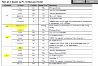
For example, I enable the gpio port E peripheral, set the GPIO_DIR register to 0xFF and begin toggling GPIO_DATA between 0x2 and 0x0. This should be toggling pin PE1 which the drawing indicates is pin 73. Instead, pin 75 toggles. Likewise, setting GPIO_DATA to 0x1 should set PE0 on pin 72, instead pin 74 toggles. This is just one example, and it appears much of Port E is scattered around on the wrong pins according to their location on the datasheet.
I've confirmed the Stellarisware and my register writes are going to the correct address per the datasheet, and this effect also happens when manipulating the peripheral registers via the CCS gui, eliminating any question about user software. To confirm I didn't have a mislabeled part, I read out the DID registers and they matched the datasheet values for the LM3S8C62.
I looked into the errata and I don't have the byte length RMW instruction pattern associated with SRAM corruption, and none of the other ones seemed relevant (although the sub-optimal reset misbehavior errata is a little worrisome).
I've also tried this on multiple LM3S8C62 devices with identical results, so I'm fairly confident there aren't any shorts or ESD related effects. This board routes the GPIO in question to LEDs+headers without any real adjacency and there are no unpowered shorts. It seems to be LM3S8C62 specific and for the life of me looks like Port E GPIO are bonded on the wrong pins.
The project is built with what I believe is the final version of the TI compiler to support the part, TI v15.12.7LTS (the assembly appears correct). I found the cells in the JTAG scan chain associated with the suspect pins, but without a BSDL file, I cannot know if these are truly misbonded or some sort of incredibly strange software issue.
Has anyone even used the LM3S8C62, or seen something remotely similar? The part doesn't exist on TI's website, although it does in CCS, and there are only a few documents scattered about.
---- UPDATE
So assuming this BSDL file is close-enough: https://bsdl.info/view.htm?sid=87280194274b27e188ca59b002289d77 there's seriously something wrong with this part's internal design. I run this code:
SysCtlPeripheralEnable(SYSCTL_PERIPH_GPIOE);
GPIOPinTypeGPIOOutput(GPIO_PORTE_BASE, GPIO_PIN_1); //0x40024000, 0x00000002
GPIOPinWrite(GPIO_PORTE_BASE, GPIO_PIN_1, GPIO_PIN_1);
Which the datasheet clearly shows in both the table and diagram that PE1 is on pin 73, but this JTAG boundary scan cell and physical pin toggles high:
"PE3_PhA1:        75, " &
...
"     1  (BC_1, *,              CONTROL,   1 ),                         " &
"     2  (BC_1, PE3_PhA1,       OUTPUT3,   X  ,      1,     1,     Z ), " &
"     3  (BC_1, PE3_PhA1,       INPUT,     X ),                         " &
This part is misbonded/datasheet is wrong?