


Part Number: AM2431
Hello,
I found these conflicting information for the datasheet and need some clarification:
- About this CAP_VDDSHV_MMC1. Which one should I trust? I don't plan to use SDIO_LDO at all but should I connect this pin directly to ground or with a 3.3uF capacitor?


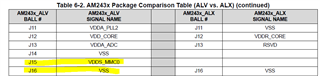
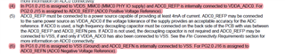
- What are the actual signal names for J15 and J16? Table 6-2 says VDDS_MMC0 and VSS but there is a note later on says it changed in "PG2.0". What are PG1.0 and PG2.0? Which should I use? They need to be connected differently in different scenarios.
Thanks,
Fang
