Part Number: AM2732
Hi.
We are currently designing a product based on AM2732, after some evaluation done on the TMDS273GPEVM. As the product is battery operated, we need to lower the power consumption of the processor in some states and have some questions around this.
Q1: If the LVDS and CSI pins/interfaces are not used (i.e. NC), can the power inputs VIOIN_18LVDS and VIOIN_18CSI power inputs be connected to GND? Does this provide any additional power save (as opposed to just disabling/clock gating these IPs from SW)?
Q2: The VPP power input voltage is specified to be 1.7V, but the current usage is not. The EVM board has a 1A LDO on this input, which seems rather strange. Do you have any specification for the current usage on this pin?
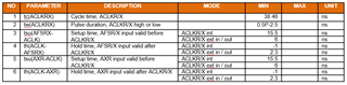
Q3: there is no timing specification for the McASP peripherals (neither in the DS nor in the TRM). Do you have any specs especially regarding the maximum bit clock rate?
Q4: In the DS (page 23) both pad V17 and pad W17 can pinmux out RCSS_MCASPC_DAT2. At the same time RCSS_MCASPC_DAT3 is not available on any pad. Is this a typo?
Q5: the LVCMOS Vih (input voltage high for LVCMOS pins) parameter for 1.8V mode is specified as 1.71V, which is the same as the minimum VIOIN value for 1.8V mode. This is practically impossible with any driving circuit if VIOIN is close to its minimum value and gives no room for noise margin. What is the real Vih for 1.8V LVCMOS inputs?
Best regards,
Paul