This thread has been locked.

If you have a related question, please click the "Ask a related question" button in the top right corner. The newly created question will be automatically linked to this question.

RM48L952: ADC group 1 readings all zero

Part Number: RM48L952
Other Parts Discussed in Thread: HALCOGEN

Hello,

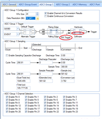
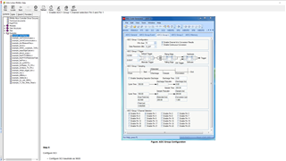
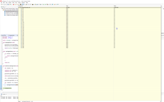
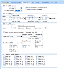
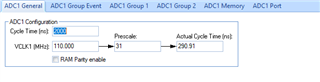
I use the ADC1 group for all 24 channels to read some external voltages. Altought the ADC1 is configured in HalCoGen to be SW triggered by GIOB0, the result is zero for all channels (there's a voltage on ADC pin , i measured it). Please find attached the configuration along with the code I try to get ADC data.

    adcStartConversion(adcREG1, adcGROUP1);

    gioSetBit(gioPORTB, 0, 1);

    while((adcIsConversionComplete(adcREG1,adcGROUP1))==0);

    gioSetBit(gioPORTB, 0, 0);

    adcGetData(adcREG1, adcGROUP1, &analogInChannels.internalAdcData[0]);

    for (channel = 0; channel < 24; channel++)
    {
        analogInChannels.volt[channel] = 0.0012210012210012 * analogInChannels.internalAdcData[channel].value;
    }

Thank you,

Best Regards,

Cosmin Briceag

  • Hi Cosmin,

    Your trigger not set to the GIOB0, and it set to the software trigger in your configuration

    And there is an example for ADC based on GIOB0 trigger in HALCoGen->Help_Topics

    there you can see step by step procedure for ADC example 

    --

    Thanks & Regards,
    Jagadish.

  • Hi,

    I followed step by step but the result is the same.

    Moreover, I got a 5V measurement on pin which does not have something attached. On the oher hand, on channel 24 I measured 2.9V but the ADC reads ZERO.

    Best Regards,

    Cosmin

  • Hi Cosmin,

    I don't have RM48 board but i tested on RM46, and i don't see any issues in ADC measurement.

    I am attaching my code here please go through it and verify.

    ADC_TEST_RM46.zip

    In this code i am reading channel 0 and 7 values of ADC1 instance and sending them to the UART.

    Also please attach your entire project, so that i can verify clearly.

    I got a 5V measurement on pin which does not have something attached

    Which board are you using, is it a ti specific one or custom one? verify in schematic whether in pull-up connected to the specific pic.

    --

    Thanks & Regards,
    Jagadish.

  • Hi Jagadish,

    Unfortunately, it does not work even with your configuration file.
    I use a custom board which does not have pull-up for ADC pins. I rephrase my sentence "I randomly get 5V on different channels".

    I attached my adc.c generated by HalCoGen.

    /** @file adc.c
    *   @brief ADC Driver Source File
    *   @date 11-Dec-2018
    *   @version 04.07.01
    *
    *   This file contains:
    *   - API Functions
    *   - Interrupt Handlers
    *   .
    *   which are relevant for the ADC driver.
    */
    
    /* 
    * Copyright (C) 2009-2018 Texas Instruments Incorporated - www.ti.com  
    * 
    * 
    *  Redistribution and use in source and binary forms, with or without 
    *  modification, are permitted provided that the following conditions 
    *  are met:
    *
    *    Redistributions of source code must retain the above copyright 
    *    notice, this list of conditions and the following disclaimer.
    *
    *    Redistributions in binary form must reproduce the above copyright
    *    notice, this list of conditions and the following disclaimer in the 
    *    documentation and/or other materials provided with the   
    *    distribution.
    *
    *    Neither the name of Texas Instruments Incorporated nor the names of
    *    its contributors may be used to endorse or promote products derived
    *    from this software without specific prior written permission.
    *
    *  THIS SOFTWARE IS PROVIDED BY THE COPYRIGHT HOLDERS AND CONTRIBUTORS 
    *  "AS IS" AND ANY EXPRESS OR IMPLIED WARRANTIES, INCLUDING, BUT NOT 
    *  LIMITED TO, THE IMPLIED WARRANTIES OF MERCHANTABILITY AND FITNESS FOR
    *  A PARTICULAR PURPOSE ARE DISCLAIMED. IN NO EVENT SHALL THE COPYRIGHT 
    *  OWNER OR CONTRIBUTORS BE LIABLE FOR ANY DIRECT, INDIRECT, INCIDENTAL, 
    *  SPECIAL, EXEMPLARY, OR CONSEQUENTIAL DAMAGES (INCLUDING, BUT NOT 
    *  LIMITED TO, PROCUREMENT OF SUBSTITUTE GOODS OR SERVICES; LOSS OF USE,
    *  DATA, OR PROFITS; OR BUSINESS INTERRUPTION) HOWEVER CAUSED AND ON ANY
    *  THEORY OF LIABILITY, WHETHER IN CONTRACT, STRICT LIABILITY, OR TORT 
    *  (INCLUDING NEGLIGENCE OR OTHERWISE) ARISING IN ANY WAY OUT OF THE USE 
    *  OF THIS SOFTWARE, EVEN IF ADVISED OF THE POSSIBILITY OF SUCH DAMAGE.
    *
    */
    
    
    /* USER CODE BEGIN (0) */
    /* USER CODE END */
    
    /* Include Files */
    
    #include "adc.h"
    #include "sys_vim.h"
    
    /* USER CODE BEGIN (1) */
    /* USER CODE END */
    
    
    /** @fn void adcInit(void)
    *   @brief Initializes ADC Driver
    *
    *   This function initializes the ADC driver.
    *
    */
    /* USER CODE BEGIN (2) */
    /* USER CODE END */
    /* SourceId : ADC_SourceId_001 */
    /* DesignId : ADC_DesignId_001 */
    /* Requirements : HL_SR185 */
    void adcInit(void)
    {
    /* USER CODE BEGIN (3) */
    /* USER CODE END */
    
        /** @b Initialize @b ADC1: */
    
        /** - Reset ADC module */
        adcREG1->RSTCR = 1U;
        adcREG1->RSTCR = 0U;
    
        /** - Enable 12-BIT ADC  */
        adcREG1->OPMODECR |= 0x80000000U;
    
        /** - Setup prescaler */
        adcREG1->CLOCKCR = 10U;
    
        /** - Setup memory boundaries */
        adcREG1->BNDCR  = (uint32)((uint32)24U << 16U) | (24U + 24U);
        adcREG1->BNDEND = (adcREG1->BNDEND & 0xFFFF0000U) | (2U);
    
        /** - Setup event group conversion mode
        *     - Setup data format
        *     - Enable/Disable channel id in conversion result
        *     - Enable/Disable continuous conversion
        */
        adcREG1->GxMODECR[0U] = (uint32)ADC_12_BIT
                              | (uint32)0x00000020U
                              | (uint32)0x00000000U;
    
        /** - Setup event group hardware trigger
         *     - Setup hardware trigger edge
         *     - Setup hardware trigger source
         */
        adcREG1->EVSRC = (uint32)0x00000008U
                       | (uint32)ADC1_GIOB0;
    
        /** - Setup event group sample window */
        adcREG1->EVSAMP = 1U;
    
        /** - Setup event group sample discharge
        *     - Setup discharge prescaler
        *     - Enable/Disable discharge
        */
        adcREG1->EVSAMPDISEN = (uint32)((uint32)0U << 8U)
                             | (uint32)0x00000000U;
    
        /** - Setup group 1 conversion mode
        *     - Setup data format
        *     - Enable/Disable channel id in conversion result
        *     - Enable/Disable continuous conversion
        */
        adcREG1->GxMODECR[1U] = (uint32)ADC_12_BIT
                              | (uint32)0x00000020U
                              | (uint32)0x00000008U
                              | (uint32)0x00000000U;
    
        /** - Setup group 1 hardware trigger
         *     - Setup hardware trigger edge
         *     - Setup hardware trigger source
         */
        adcREG1->G1SRC = (uint32)0x00000008U
                       | (uint32)ADC1_GIOB0;
    
        /** - Setup group 1 sample window */
        adcREG1->G1SAMP = 1U;
    
        /** - Setup group 1 sample discharge
        *     - Setup discharge prescaler
        *     - Enable/Disable discharge
        */
        adcREG1->G1SAMPDISEN = (uint32)((uint32)0U << 8U)
                             | (uint32)0x00000000U;
    
        /** - Setup group 2 conversion mode
         *     - Setup data format
         *     - Enable/Disable channel id in conversion result
         *     - Enable/Disable continuous conversion
         */
        adcREG1->GxMODECR[2U] = (uint32)ADC_12_BIT
                              | (uint32)0x00000000U
                              | (uint32)0x00000008U
                              | (uint32)0x00000000U;
    
        /** - Setup group 2 hardware trigger
        *     - Setup hardware trigger edge
        *     - Setup hardware trigger source
        */
        adcREG1->G2SRC = (uint32)0x00000008U
                       | (uint32)ADC1_EVENT;
    
        /** - Setup group 2 sample window */
        adcREG1->G2SAMP = 1U;
    
        /** - Setup group 2 sample discharge
        *     - Setup discharge prescaler
        *     - Enable/Disable discharge
        */
        adcREG1->G2SAMPDISEN = (uint32)((uint32)0U << 8U)
                             | (uint32)0x00000000U;
    
        /** - ADC1 EVT pin output value */
        adcREG1->EVTOUT = 0U;
    
        /** - ADC1 EVT pin direction */
        adcREG1->EVTDIR = 0U;
    
        /** - ADC1 EVT pin open drain enable */
        adcREG1->EVTPDR = 0U;
    
        /** - ADC1 EVT pin pullup / pulldown selection */
        adcREG1->EVTPSEL = 1U;
    
        /** - ADC1 EVT pin pullup / pulldown enable*/
        adcREG1->EVTDIS = 0U;
    
        /** - Enable ADC module */
        adcREG1->OPMODECR |= 0x80140001U;
    
        /** - Wait for buffer initialization complete */
        /*SAFETYMCUSW 28 D MR:NA <APPROVED> "Hardware status bit read check" */
        while (((adcREG1->BNDEND & 0xFFFF0000U) >> 16U ) != 0U)
        {
        } /* Wait */
    
        /** - Setup parity */
        adcREG1->PARCR = 0x00000005U;
    
    
    /* USER CODE BEGIN (4) */
    /* USER CODE END */
    }
    
    /* USER CODE BEGIN (5) */
    /* USER CODE END */
    
    
    /** - s_adcSelect is used as constant table for channel selection */
    static const uint32 s_adcSelect[2U][3U] =
    {
        {0x00000000U |
        0x00000000U |
        0x00000000U |
        0x00000000U |
        0x00000000U |
        0x00000000U |
        0x00000000U |
        0x00000000U |
        0x00000000U |
        0x00000000U |
        0x00000000U |
        0x00000000U |
        0x00000000U |
        0x00000000U |
        0x00000000U |
        0x00000000U |
        0x00000000U |
        0x00000000U |
        0x00000000U |
        0x00000000U |
        0x00000000U |
        0x00000000U |
        0x00000000U |
        0x00000000U,
        0x00000001U |
        0x00000002U |
        0x00000004U |
        0x00000008U |
        0x00000010U |
        0x00000020U |
        0x00000040U |
        0x00000080U |
        0x00000100U |
        0x00000200U |
        0x00000400U |
        0x00000800U |
        0x00001000U |
        0x00002000U |
        0x00004000U |
        0x00008000U |
        0x00010000U |
        0x00020000U |
        0x00040000U |
        0x00080000U |
        0x00100000U |
        0x00200000U |
        0x00400000U |
        0x00800000U,
        0x00000000U |
        0x00000000U |
        0x00000000U |
        0x00000000U |
        0x00000000U |
        0x00000000U |
        0x00000000U |
        0x00000000U |
        0x00000000U |
        0x00000000U |
        0x00000000U |
        0x00000000U |
        0x00000000U |
        0x00000000U |
        0x00000000U |
        0x00000000U |
        0x00000000U |
        0x00000000U |
        0x00000000U |
        0x00000000U |
        0x00000000U |
        0x00000000U |
        0x00000000U |
        0x00000000U},
        {0x00000000U |
        0x00000000U |
        0x00000000U |
        0x00000000U |
        0x00000000U |
        0x00000000U |
        0x00000000U |
        0x00000000U |
        0x00000000U |
        0x00000000U |
        0x00000000U |
        0x00000000U |
        0x00000000U |
        0x00000000U |
        0x00000000U |
        0x00000000U ,
        0x00000000U |
        0x00000000U |
        0x00000000U |
        0x00000000U |
        0x00000000U |
        0x00000000U |
        0x00000000U |
        0x00000000U |
        0x00000000U |
        0x00000000U |
        0x00000000U |
        0x00000000U |
        0x00000000U |
        0x00000000U |
        0x00000000U |
        0x00000000U,
        0x00000000U |
        0x00000000U |
        0x00000000U |
        0x00000000U |
        0x00000000U |
        0x00000000U |
        0x00000000U |
        0x00000000U |
        0x00000000U |
        0x00000000U |
        0x00000000U |
        0x00000000U |
        0x00000000U |
        0x00000000U |
        0x00000000U |
        0x00000000U}
    };
    
    /** - s_adcFiFoSize is used as constant table for channel selection */
    static const uint32 s_adcFiFoSize[2U][3U] =
    {
        {24U,
        24U,
        16U},
        {16U,
        16U,
        16U}
    };
    
    /* USER CODE BEGIN (6) */
    /* USER CODE END */
    
    /** @fn void adcStartConversion(adcBASE_t *adc, uint32 group)
    *   @brief Starts an ADC conversion
    *   @param[in] adc Pointer to ADC module:
    *              - adcREG1: ADC1 module pointer
    *              - adcREG2: ADC2 module pointer
    *   @param[in] group Hardware group of ADC module:
    *              - adcGROUP0: ADC event group
    *              - adcGROUP1: ADC group 1
    *              - adcGROUP2: ADC group 2
    *
    *   This function starts a conversion of the ADC hardware group.
    *
    */
    /* SourceId : ADC_SourceId_002 */
    /* DesignId : ADC_DesignId_002 */
    /* Requirements : HL_SR186 */
    void adcStartConversion(adcBASE_t *adc, uint32 group)
    {
        uint32 index = (adc == adcREG1) ? 0U : 1U;
    
    /* USER CODE BEGIN (7) */
    /* USER CODE END */
    
        /** - Setup FiFo size */
        adc->GxINTCR[group] = s_adcFiFoSize[index][group];
    
        /** - Start Conversion */
        adc->GxSEL[group] = s_adcSelect[index][group];
    
        /**   @note The function adcInit has to be called before this function can be used. */
    
    /* USER CODE BEGIN (8) */
    /* USER CODE END */
    }
    
    /* USER CODE BEGIN (9) */
    /* USER CODE END */
    
    
    /** @fn void adcStopConversion(adcBASE_t *adc, uint32 group)
    *   @brief Stops an ADC conversion
    *   @param[in] adc Pointer to ADC module:
    *              - adcREG1: ADC1 module pointer
    *              - adcREG2: ADC2 module pointer
    *   @param[in] group Hardware group of ADC module:
    *              - adcGROUP0: ADC event group
    *              - adcGROUP1: ADC group 1
    *              - adcGROUP2: ADC group 2
    *
    *   This function stops a conversion of the ADC hardware group.
    *
    */
    /* SourceId : ADC_SourceId_003 */
    /* DesignId : ADC_DesignId_003 */
    /* Requirements : HL_SR187 */
    void adcStopConversion(adcBASE_t *adc, uint32 group)
    {
    /* USER CODE BEGIN (10) */
    /* USER CODE END */
    
        /** - Stop Conversion */
        adc->GxSEL[group] = 0U;
    
        /**   @note The function adcInit has to be called before this function can be used. */
    
    /* USER CODE BEGIN (11) */
    /* USER CODE END */
    }
    
    /* USER CODE BEGIN (12) */
    /* USER CODE END */
    
    
    /** @fn void adcResetFiFo(adcBASE_t *adc, uint32 group)
    *   @brief Resets FiFo read and write pointer.
    *   @param[in] adc Pointer to ADC module:
    *              - adcREG1: ADC1 module pointer
    *              - adcREG2: ADC2 module pointer
    *   @param[in] group Hardware group of ADC module:
    *              - adcGROUP0: ADC event group
    *              - adcGROUP1: ADC group 1
    *              - adcGROUP2: ADC group 2
    *
    *   This function resets the FiFo read and write pointers.
    *
    */
    /* SourceId : ADC_SourceId_004 */
    /* DesignId : ADC_DesignId_004*/
    /* Requirements : HL_SR188 */
    void adcResetFiFo(adcBASE_t *adc, uint32 group)
    {
    /* USER CODE BEGIN (13) */
    /* USER CODE END */
    
        /** - Reset FiFo */
        adc->GxFIFORESETCR[group] = 1U;
    
        /**   @note The function adcInit has to be called before this function can be used.\n
        *           the conversion should be stopped before calling this function.
        */
    
    /* USER CODE BEGIN (14) */
    /* USER CODE END */
    }
    
    /* USER CODE BEGIN (15) */
    /* USER CODE END */
    
    
    /** @fn uint32 adcGetData(adcBASE_t *adc, uint32 group, adcData_t * data)
    *   @brief Gets converted a ADC values
    *   @param[in] adc Pointer to ADC module:
    *              - adcREG1: ADC1 module pointer
    *              - adcREG2: ADC2 module pointer
    *   @param[in] group Hardware group of ADC module:
    *              - adcGROUP0: ADC event group
    *              - adcGROUP1: ADC group 1
    *              - adcGROUP2: ADC group 2
    *   @param[out] data Pointer to store ADC converted data
    *   @return The function will return the number of converted values copied into data buffer:
    *
    *   This function writes a ADC message into a ADC message box.
    *
    */
    /* SourceId : ADC_SourceId_005 */
    /* DesignId : ADC_DesignId_005 */
    /* Requirements : HL_SR189 */
    uint32 adcGetData(adcBASE_t *adc, uint32 group, adcData_t * data)
    {
        uint32       i;
        uint32  buf;
        uint32  mode;
        uint32  index = (adc == adcREG1) ? 0U : 1U;
    
    	uint32  intcr_reg = adc->GxINTCR[group];
        uint32  count = (intcr_reg >= 256U) ? s_adcFiFoSize[index][group] : (s_adcFiFoSize[index][group] - (uint32)(intcr_reg & 0xFFU));
        adcData_t *ptr = data;
    
    /* USER CODE BEGIN (16) */
    /* USER CODE END */
    
        mode = (adc->OPMODECR & ADC_12_BIT_MODE);
    
        if(mode == ADC_12_BIT_MODE)
          {
            /** -  Get conversion data and channel/pin id */
            for (i = 0U; i < count; i++)
            {
              buf        = adc->GxBUF[group].BUF0;
              /*SAFETYMCUSW 45 D MR:21.1 <APPROVED> "Valid non NULL input parameters are only allowed in this driver" */
              ptr->value = (uint16)(buf & 0xFFFU);
              ptr->id    = (uint32)((buf >> 16U) & 0x1FU);
              /*SAFETYMCUSW 567 S MR:17.1,17.4 <APPROVED> "Pointer increment needed" */
              ptr++;
            }
          }
          else
          {
            /** -  Get conversion data and channel/pin id */
            for (i = 0U; i < count; i++)
            {
              buf        = adc->GxBUF[group].BUF0;
              /*SAFETYMCUSW 45 D MR:21.1 <APPROVED> "Valid non NULL input parameters are only allowed in this driver" */
              ptr->value = (uint16)(buf & 0x3FFU);
              ptr->id    = (uint32)((buf >> 10U) & 0x1FU);
              /*SAFETYMCUSW 567 S MR:17.1,17.4 <APPROVED> "Pointer increment needed" */
              ptr++;
            }
          }
    
    
        adc->GxINTFLG[group] = 9U;
    
        /**   @note The function adcInit has to be called before this function can be used.\n
        *           The user is responsible to initialize the message box.
        */
    
    /* USER CODE BEGIN (17) */
    /* USER CODE END */
    
        return count;
    }
    
    /* USER CODE BEGIN (18) */
    /* USER CODE END */
    
    
    /** @fn uint32 adcIsFifoFull(adcBASE_t *adc, uint32 group)
    *   @brief Checks if FiFo buffer is full
    *   @param[in] adc Pointer to ADC module:
    *              - adcREG1: ADC1 module pointer
    *              - adcREG2: ADC2 module pointer
    *   @param[in] group Hardware group of ADC module:
    *              - adcGROUP0: ADC event group
    *              - adcGROUP1: ADC group 1
    *              - adcGROUP2: ADC group 2
    *   @return The function will return:
    *           - 0: When FiFo buffer is not full
    *           - 1: When FiFo buffer is full
    *           - 3: When FiFo buffer overflow occurred
    *
    *   This function checks FiFo buffer status.
    *
    */
    /* SourceId : ADC_SourceId_006 */
    /* DesignId : ADC_DesignId_006 */
    /* Requirements : HL_SR190 */
    uint32 adcIsFifoFull(adcBASE_t *adc, uint32 group)
    {
        uint32 flags;
    
    /* USER CODE BEGIN (19) */
    /* USER CODE END */
    
        /** - Read FiFo flags */
        flags = adc->GxINTFLG[group] & 3U;
    
        /**   @note The function adcInit has to be called before this function can be used. */
    
    /* USER CODE BEGIN (20) */
    /* USER CODE END */
    
        return flags;
    }
    
    /* USER CODE BEGIN (21) */
    /* USER CODE END */
    
    
    /** @fn uint32 adcIsConversionComplete(adcBASE_t *adc, uint32 group)
    *   @brief Checks if Conversion is complete
    *   @param[in] adc Pointer to ADC module:
    *              - adcREG1: ADC1 module pointer
    *              - adcREG2: ADC2 module pointer
    *   @param[in] group Hardware group of ADC module:
    *              - adcGROUP0: ADC event group
    *              - adcGROUP1: ADC group 1
    *              - adcGROUP2: ADC group 2
    *   @return The function will return:
    *           - 0: When is not finished
    *           - 8: When conversion is complete
    *
    *   This function checks if conversion is complete.
    *
    */
    /* SourceId : ADC_SourceId_007 */
    /* DesignId : ADC_DesignId_007 */
    /* Requirements : HL_SR191 */
    uint32 adcIsConversionComplete(adcBASE_t *adc, uint32 group)
    {
        uint32 flags;
    
    /* USER CODE BEGIN (22) */
    /* USER CODE END */
    
        /** - Read conversion flags */
        flags = adc->GxINTFLG[group] & 8U;
    
        /**   @note The function adcInit has to be called before this function can be used. */
    
    /* USER CODE BEGIN (23) */
    /* USER CODE END */
    
        return flags;
    }
    
    /* USER CODE BEGIN (24) */
    /* USER CODE END */
    
    /** @fn void adcCalibration(adcBASE_t *adc)
    *   @brief Computes offset error using Calibration mode
    *   @param[in] adc Pointer to ADC module:
    *              - adcREG1: ADC1 module pointer
    *              - adcREG2: ADC2 module pointer
    *   This function computes offset error using Calibration mode
    *
    */
    /* SourceId : ADC_SourceId_008 */
    /* DesignId : ADC_DesignId_010 */
    /* Requirements : HL_SR194 */
    void adcCalibration(adcBASE_t *adc)
    {
    /* USER CODE BEGIN (25) */
    /* USER CODE END */
    
        uint32 conv_val[5U]={0U,0U,0U,0U,0U};
        uint32 loop_index=0U;
        uint32 offset_error=0U;
        uint32 backup_mode;
    
        /** - Backup Mode before Calibration  */
        backup_mode = adc->OPMODECR;
    
        /** - Enable 12-BIT ADC  */
        adc->OPMODECR |= 0x80000000U;
    
        /* Disable all channels for conversion */
        adc->GxSEL[0U]=0x00U;
        adc->GxSEL[1U]=0x00U;
        adc->GxSEL[2U]=0x00U;
    
        for(loop_index=0U;loop_index<4U;loop_index++)
        {
            /* Disable Self Test and Calibration mode */
            adc->CALCR=0x0U;
    
            switch(loop_index)
            {
                case 0U :   /* Test 1 : Bride En = 0 , HiLo =0 */
                            adc->CALCR=0x0U;
                            break;
    
                case 1U :   /* Test 1 : Bride En = 0 , HiLo =1 */
                            adc->CALCR=0x0100U;
                            break;
    
                case 2U :   /* Test 1 : Bride En = 1 , HiLo =0 */
                            adc->CALCR=0x0200U;
                            break;
    
                case 3U :   /* Test 1 : Bride En = 1 , HiLo =1 */
                            adc->CALCR=0x0300U;
                            break;
                default :
                            break;
            }
    
            /* Enable Calibration mode */
            adc->CALCR|=0x1U;
    
            /* Start calibration conversion */
            adc->CALCR|=0x00010000U;
    
            /* Wait for calibration conversion to complete */
            /*SAFETYMCUSW 28 D MR:NA <APPROVED> "Hardware status bit read check" */
            while((adc->CALCR & 0x00010000U)==0x00010000U)
            {
            } /* Wait */
    
            /* Read converted value */
            conv_val[loop_index]= adc->CALR;
        }
    
        /* Disable Self Test and Calibration mode */
        adc->CALCR=0x0U;
    
        /* Compute the Offset error correction value */
        conv_val[4U]=conv_val[0U]+ conv_val[1U] + conv_val[2U] + conv_val[3U];
    
        conv_val[4U]=(conv_val[4U]/4U);
    
        offset_error=conv_val[4U]-0x7FFU;
    
        /*Write the offset error to the Calibration register */
        /* Load 2;s complement of the computed value to ADCALR register */
        offset_error=~offset_error;
        offset_error=offset_error & 0xFFFU;
        offset_error=offset_error+1U;
    
        adc->CALR = offset_error;
    
      /** - Restore Mode after Calibration  */
        adc->OPMODECR = backup_mode;
    
     /**   @note The function adcInit has to be called before using this function. */
    
    /* USER CODE BEGIN (26) */
    /* USER CODE END */
    }
    
    
    /** @fn void adcMidPointCalibration(adcBASE_t *adc)
    *   @brief Computes offset error using Mid Point Calibration mode
    *   @param[in] adc Pointer to ADC module:
    *              - adcREG1: ADC1 module pointer
    *              - adcREG2: ADC2 module pointer
    *   @return This function will return offset error using Mid Point Calibration mode
    *
    *   This function computes offset error using Mid Point Calibration mode
    *
    */
    /* SourceId : ADC_SourceId_009 */
    /* DesignId : ADC_DesignId_011 */
    /* Requirements : HL_SR195 */
    uint32 adcMidPointCalibration(adcBASE_t *adc)
    {
    /* USER CODE BEGIN (27) */
    /* USER CODE END */
    
        uint32 conv_val[3U]={0U,0U,0U};
        uint32 loop_index=0U;
        uint32 offset_error=0U;
        uint32 backup_mode;
    
        /** - Backup Mode before Calibration  */
        backup_mode = adc->OPMODECR;
    
        /** - Enable 12-BIT ADC  */
        adc->OPMODECR |= 0x80000000U;
    
        /* Disable all channels for conversion */
        adc->GxSEL[0U]=0x00U;
        adc->GxSEL[1U]=0x00U;
        adc->GxSEL[2U]=0x00U;
    
        for(loop_index=0U;loop_index<2U;loop_index++)
        {
            /* Disable Self Test and Calibration mode */
            adc->CALCR=0x0U;
    
            switch(loop_index)
            {
                case 0U :   /* Test 1 : Bride En = 0 , HiLo =0 */
                            adc->CALCR=0x0U;
                            break;
    
                case 1U :   /* Test 1 : Bride En = 0 , HiLo =1 */
                            adc->CALCR=0x0100U;
                            break;
    
                default :
                            break;
    
            }
    
            /* Enable Calibration mode */
            adc->CALCR|=0x1U;
    
            /* Start calibration conversion */
            adc->CALCR|=0x00010000U;
    
            /* Wait for calibration conversion to complete */
            /*SAFETYMCUSW 28 D MR:NA <APPROVED> "Hardware status bit read check" */
            while((adc->CALCR & 0x00010000U)==0x00010000U)
            {
            } /* Wait */
    
            /* Read converted value */
            conv_val[loop_index]= adc->CALR;
        }
    
        /* Disable Self Test and Calibration mode */
        adc->CALCR=0x0U;
    
        /* Compute the Offset error correction value */
        conv_val[2U]=(conv_val[0U])+ (conv_val[1U]);
    
        conv_val[2U]=(conv_val[2U]/2U);
    
        offset_error=conv_val[2U]-0x7FFU;
    
        /* Write the offset error to the Calibration register           */
        /* Load 2's complement of the computed value to ADCALR register */
        offset_error=~offset_error;
        offset_error=offset_error+1U;
        offset_error=offset_error & 0xFFFU;
    
        adc->CALR = offset_error;
    
      /** - Restore Mode after Calibration  */
        adc->OPMODECR = backup_mode;
    
        return(offset_error);
    
     /**   @note The function adcInit has to be called before this function can be used. */
    
    /* USER CODE BEGIN (28) */
    /* USER CODE END */
    }
    
    /* USER CODE BEGIN (29) */
    /* USER CODE END */
    
    /** @fn void adcEnableNotification(adcBASE_t *adc, uint32 group)
    *   @brief Enable notification
    *   @param[in] adc Pointer to ADC module:
    *              - adcREG1: ADC1 module pointer
    *              - adcREG2: ADC2 module pointer
    *   @param[in] group Hardware group of ADC module:
    *              - adcGROUP0: ADC event group
    *              - adcGROUP1: ADC group 1
    *              - adcGROUP2: ADC group 2
    *
    *   This function will enable the notification of a conversion.
    *   In single conversion mode for conversion complete and
    *   in continuous conversion mode when the FiFo buffer is full.
    *
    */
    /* SourceId : ADC_SourceId_010 */
    /* DesignId : ADC_DesignId_008 */
    /* Requirements : HL_SR192 */
    void adcEnableNotification(adcBASE_t *adc, uint32 group)
    {
        uint32 notif = (((uint32)(adc->GxMODECR[group]) & 2U) == 2U) ? 1U : 8U;
    
    /* USER CODE BEGIN (30) */
    /* USER CODE END */
    
        adc->GxINTENA[group] = notif;
    
        /**   @note The function adcInit has to be called before this function can be used.\n
        *           This function should be called before the conversion is started
        */
    
    /* USER CODE BEGIN (31) */
    /* USER CODE END */
    }
    
    /* USER CODE BEGIN (32) */
    /* USER CODE END */
    
    
    /** @fn void adcDisableNotification(adcBASE_t *adc, uint32 group)
    *   @brief Disable notification
    *   @param[in] adc Pointer to ADC module:
    *              - adcREG1: ADC1 module pointer
    *              - adcREG2: ADC2 module pointer
    *   @param[in] group Hardware group of ADC module:
    *              - adcGROUP0: ADC event group
    *              - adcGROUP1: ADC group 1
    *              - adcGROUP2: ADC group 2
    *
    *   This function will disable the notification of a conversion.
    */
    /* SourceId : ADC_SourceId_011 */
    /* DesignId : ADC_DesignId_009 */
    /* Requirements : HL_SR193 */
    void adcDisableNotification(adcBASE_t *adc, uint32 group)
    {
    /* USER CODE BEGIN (33) */
    /* USER CODE END */
    
        adc->GxINTENA[group] = 0U;
    
        /**   @note The function adcInit has to be called before this function can be used. */
    
    /* USER CODE BEGIN (34) */
    /* USER CODE END */
    }
    
    /** @fn void adcSetEVTPin(adcBASE_t *adc, uint32 value)
    *   @brief Set ADCEVT pin
    *   @param[in] adc Pointer to ADC module:
    *              - adcREG1: ADC1 module pointer
    *   @param[in] value Value to be set: 0 or 1
    *
    *   This function will set the ADC EVT pin if configured as an output pin.
    */
    /* SourceId : ADC_SourceId_020 */
    /* DesignId : ADC_DesignId_014 */
    /* Requirements : HL_SR529 */
    void adcSetEVTPin(adcBASE_t *adc, uint32 value)
    {
        adc->EVTOUT = value;
    }
    
    /** @fn uint32 adcGetEVTPin(adcBASE_t *adc)
    *   @brief Set ADCEVT pin
    *   @param[in] adc Pointer to ADC module:
    *              - adcREG1: ADC1 module pointer
    *   @return Value of the ADC EVT pin: 0 or 1
    *
    *   This function will return the value of ADC EVT pin.
    */
    /* SourceId : ADC_SourceId_021 */
    /* DesignId : ADC_DesignId_015 */
    /* Requirements : HL_SR529 */
    uint32 adcGetEVTPin(adcBASE_t *adc)
    {
        return adc->EVTIN;
    }
    
    /** @fn void adc1GetConfigValue(adc_config_reg_t *config_reg, config_value_type_t type)
    *   @brief Get the initial or current values of the configuration registers
    *
    *   @param[in] *config_reg: pointer to the struct to which the initial or current
    *                           value of the configuration registers need to be stored
    *   @param[in] type:    whether initial or current value of the configuration registers need to be stored
    *                       - InitialValue: initial value of the configuration registers will be stored
    *                                       in the struct pointed by config_reg
    *                       - CurrentValue: initial value of the configuration registers will be stored
    *                                       in the struct pointed by config_reg
    *
    *   This function will copy the initial or current value (depending on the parameter 'type')
    *   of the configuration registers to the struct pointed by config_reg
    *
    */
    /* SourceId : ADC_SourceId_012 */
    /* DesignId : ADC_DesignId_012 */
    /* Requirements : HL_SR203 */
    void adc1GetConfigValue(adc_config_reg_t *config_reg, config_value_type_t type)
    {
        if (type == InitialValue)
        {
            config_reg->CONFIG_OPMODECR = ADC1_OPMODECR_CONFIGVALUE;
            config_reg->CONFIG_CLOCKCR = ADC1_CLOCKCR_CONFIGVALUE;
            config_reg->CONFIG_GxMODECR[0U] = ADC1_G0MODECR_CONFIGVALUE;
            config_reg->CONFIG_GxMODECR[1U] = ADC1_G1MODECR_CONFIGVALUE;
            config_reg->CONFIG_GxMODECR[2U] = ADC1_G2MODECR_CONFIGVALUE;
            config_reg->CONFIG_G0SRC = ADC1_G0SRC_CONFIGVALUE;
            config_reg->CONFIG_G1SRC = ADC1_G1SRC_CONFIGVALUE;
            config_reg->CONFIG_G2SRC = ADC1_G2SRC_CONFIGVALUE;
            config_reg->CONFIG_BNDCR = ADC1_BNDCR_CONFIGVALUE;
            config_reg->CONFIG_BNDEND = ADC1_BNDEND_CONFIGVALUE;
            config_reg->CONFIG_G0SAMP = ADC1_G0SAMP_CONFIGVALUE;
            config_reg->CONFIG_G1SAMP = ADC1_G1SAMP_CONFIGVALUE;
            config_reg->CONFIG_G2SAMP = ADC1_G2SAMP_CONFIGVALUE;
            config_reg->CONFIG_G0SAMPDISEN = ADC1_G0SAMPDISEN_CONFIGVALUE;
            config_reg->CONFIG_G1SAMPDISEN = ADC1_G1SAMPDISEN_CONFIGVALUE;
            config_reg->CONFIG_G2SAMPDISEN = ADC1_G2SAMPDISEN_CONFIGVALUE;
            config_reg->CONFIG_PARCR = ADC1_PARCR_CONFIGVALUE;
        }
        else
        {
            config_reg->CONFIG_OPMODECR = adcREG1->OPMODECR;
            config_reg->CONFIG_CLOCKCR = adcREG1->CLOCKCR;
            config_reg->CONFIG_GxMODECR[0U] = adcREG1->GxMODECR[0U];
            config_reg->CONFIG_GxMODECR[1U] = adcREG1->GxMODECR[1U];
            config_reg->CONFIG_GxMODECR[2U] = adcREG1->GxMODECR[2U];
            config_reg->CONFIG_G0SRC = adcREG1->EVSRC;
            config_reg->CONFIG_G1SRC = adcREG1->G1SRC;
            config_reg->CONFIG_G2SRC = adcREG1->G2SRC;
            config_reg->CONFIG_BNDCR = adcREG1->BNDCR;
            config_reg->CONFIG_BNDEND = adcREG1->BNDEND;
            config_reg->CONFIG_G0SAMP = adcREG1->EVSAMP;
            config_reg->CONFIG_G1SAMP = adcREG1->G1SAMP;
            config_reg->CONFIG_G2SAMP = adcREG1->G2SAMP;
            config_reg->CONFIG_G0SAMPDISEN = adcREG1->EVSAMPDISEN;
            config_reg->CONFIG_G1SAMPDISEN = adcREG1->G1SAMPDISEN;
            config_reg->CONFIG_G2SAMPDISEN = adcREG1->G2SAMPDISEN;
            config_reg->CONFIG_PARCR = adcREG1->PARCR;
        }
    }
    
    
    /* USER CODE BEGIN (35) */
    /* USER CODE END */
    
    /** @fn void adc1Group0Interrupt(void)
    *   @brief ADC1 Event Group Interrupt Handler
    */
    #pragma CODE_STATE(adc1Group0Interrupt, 32)
    #pragma INTERRUPT(adc1Group0Interrupt, IRQ)
    
    /* SourceId : ADC_SourceId_014 */
    /* DesignId : ADC_DesignId_013 */
    /* Requirements : HL_SR197, HL_SR196 */
    void adc1Group0Interrupt(void)
    {
    /* USER CODE BEGIN (36) */
    /* USER CODE END */
    
        adcREG1->GxINTFLG[0U] = 9U;
    
        adcNotification(adcREG1, adcGROUP0);
    
    /* USER CODE BEGIN (37) */
    /* USER CODE END */
    }
    
    /* USER CODE BEGIN (38) */
    /* USER CODE END */
    /** @fn void adc1Group1Interrupt(void)
    *   @brief ADC1 Group 1 Interrupt Handler
    */
    #pragma CODE_STATE(adc1Group1Interrupt, 32)
    #pragma INTERRUPT(adc1Group1Interrupt, IRQ)
    
    /* SourceId : ADC_SourceId_015 */
    /* DesignId : ADC_DesignId_013 */
    /* Requirements : HL_SR197, HL_SR196 */
    void adc1Group1Interrupt(void)
    {
    /* USER CODE BEGIN (39) */
    /* USER CODE END */
    
        adcREG1->GxINTFLG[1U] = 9U;
    
        adcNotification(adcREG1, adcGROUP1);
    
    /* USER CODE BEGIN (40) */
    /* USER CODE END */
    }


    Best Regads,

    Cosmin

  • Hi Cosmin,

    only adc.c may not helpful, 

    Can you please zip your entire project and attach it?

    --
    Thanks & Regards,
    Jagadish.

  • Hi,

    The whole project is not relevant for ADC, I attached only the generated files along with the halcogen .cfg file which should be enough for detecting any missconfiguration.

     mcal.zip

  • Hi Cosmin,

    I verified your ADC initialization, and it looks fine. But i don't find where you are calling the functions adcInit and adcStartConversion functions in your code

    Please make sure you are calling adcStartConversion function, before giving rising edge on GIOB0.

    --

    Thanks & Regards,
    Jagadish.

  • Hi Jagadish,

    I call them properly, please have a look at the yelow picture. 

    Cosmin,

  • Hi Coosmin,

    Okay, but where you are calling "adcInit" function in your application?

    --
    Thanks & Regards,
    Jagadish.

  • it is called inside halInit()...along with the analogInInit()...

  • Okay, that is good.

    One more question, from where "adcInternalAcquired" is calling? because in this function only right we are giving rising edge trigger to the ADC.

  • void halInit(void)
    {
        [...]
        adcInit();
        analogInInit();
        [...]
    
    //test code
        while(1)
        {
            adcInternalAcquired();
        }
    }

  • Hi Cosmin,

    Your code looks fine for me,

    can you please do one thing?  

    After calling gio set direction function in analogInInit function, can you please also call the below function?

    gioSetBit(gioPORTB, 0, 0);

    This function makes sure the gioB0 pin value to zero, so after calling gio set function with value 1 in adcinternalacquired a rising edge will be created.

    Do above modification and test it.

    --

    Thanks & Regards,
    Jagadish.

  • Hi,

    It does not work.

    Cosmin,

  • Hi, 

    I think I got a HW issue, pins ADREFHI and ADREFLO are floating....I'll fix them and come back with the result.

    Best Regards,

    Cosmin

  • I connected ADREFHI to 5V and ADREFLO to GND and now i get 4095 raw value for each ADC channel....What is wrong ?

  • Hi Cosmin,

    I thought is a software bug but good to know you found issue related to hardware

    What is wrong ?

    Did you connect the 5V to VCCAD or not?

    It is also mandatory to connect supply to the VCCAD pin to function ADC properly.

    --

    Thanks & Regards,
    Jagadish.

  • Hello,

    Yes, VCCAD is connected to 5V.

    Thank you.

    Cosmin

  • Yes, VCCAD is connected to 5V.

    So, that means you are reading 4095 for all channels even after connecting 5V to VCCAD also, right?

    And what if some voltage connected to ADC pin, are you getting corresponding digital for that analog input or still you are reading 4095 for those pins also?

    --

    Thanks & Regards,
    Jagadish.

  • Yes, I read 4095 for all channels although the actual voltage is zero (measured).

  • Hi Cosmin,

    Reading 4095 on all ADC channels will be possible in below condition only

    Either not properly connecting 5V to ADREFHI or GND to ADREFLO.

    Example:

    If ADREFHI not properly connected to 5V and assume that it is connected to ground in that case all pin voltages are greater than or equal to ADREFHI right (even pins are unconnected) so all channels can read 4095.

    So can you please make sure again, that a 5V connected to ADREFHI and GND is connected to the ADREFLO.

    --

    Thanks & Regards,
    Jagadish.

  • Hello Jagadish,

    It was proven to be a fault in HW. Thank you very much for your help.

    Best Regards,

    Cosmin

  • It was proven to be a fault in HW

    Any idea what exactly the fault?

  • weel, the op amp used to measure some currents was saturated. Although initially there was no voltage on ADC pin.