This thread has been locked.

If you have a related question, please click the "Ask a related question" button in the top right corner. The newly created question will be automatically linked to this question.

TMS570LC4357: HET not initializing after POR

Part Number: TMS570LC4357

Hello,

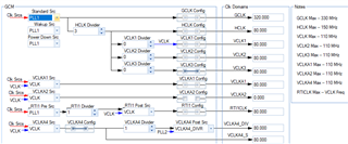
I am facing a problem where the HET is not Initializing after a Power on Reset. This does not happen after every POR but happens quite often.

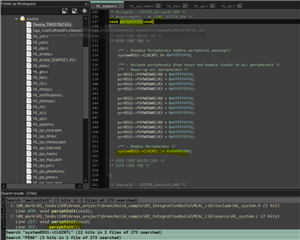
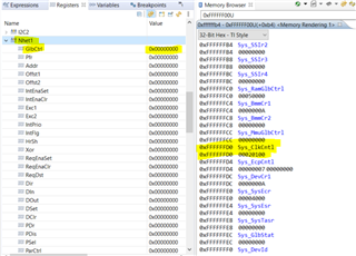
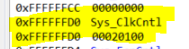
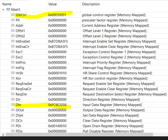
The below Picture is in case of normal HET Initialization where HET Hardware is ON and Data can be seen in the DIN Register.

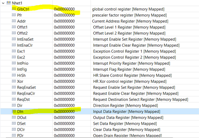
The below Picture is in case of abnormal HET Initialization where HET Hardware is OFF and Data cannot be seen in the DIN Register. We can recover from this Problem by doing a POR.

Can you please assist me in this Issue.

Kind Regards,

Sakti

  • Hi Sakti,

    To use the HET module, the module should be released from power down which enables clock to HET module. This step is done by following code in periphInit(void) function of HL_system.c

     pcrREG->PSPWRDWNCLRxxx = 0xFFFFFFFFU;

    and 

    set PENA bit of  systemREG1->CLKCNTL

    After the module is powered on, you can program the NHET registers.

  • Hello Wang,

    Thank you for a quick Response.

    pcrREG->PSPWRDWNCLRxxx = 0xFFFFFFFFU;

    and 

    set PENA bit of  systemREG1->CLKCNTL

    These are executed in the code by default as you said in the HL_system.c File.

    Any other Possibility why this Issue can happen. This issue does not happen on every POR but does happen quite often.

    Regards

  • Please double check if PENA bit is set. Can other modules for example GIOA and GIOB be used?

  • Hello,

    Yes, The PENA bit is set but the HET Registers are not updating as seen in the Picture below.

    Yes, GIO can be used. I am using GIO to blink a LED periodically in the Code and that's happening.

    Regards

  • After PENA is set, the N2HET registers should be programmable. 

    The VCLK2 in your configuration is HCLK/1. What is HCLK? The maximum frequency of VCLK2 is 110MHz.

  • This is my Clock Configuration.

    My HCLK Clock is configured to 240MHz but the max is 150MHz. Maybe this is problem.

    Regards

  • Hi Sakti,

    240MHz is out of the valid range. Have you tried the slower system clock, 150MHz, 120MHz etc?

  • Hello,

    I think the Issue is resolved after adjusting the Clock of HCLK to 150MHz (Max allowed clock)

    .I wanted to check If the HCLK is set at 240 MHz, What would be the Clock frequency operate at?? Would the system operate at 150MHz(Max allowed frequency) or at 240MHz???

    Regards

  • Hello Wang,

    A couple of more Questions: -

    1. I can see that HCLK effects the L2RAM and FEE Clock. What would be the effects on these Peripherals if the HCLK frequency is reduced?? What would be the recommended and maximum L2RAM and FEE clock frequency??

    2. What is the HCLK (System Clock) used for in the Microcontroller?? Which other Peripherals are driven by HCLK and what would be the effect on the System in case HCLK frequency is reduced?

    Thanks

  • Hello, 

    Also wanted to check with you an Ideal clock configuration possible to meet the requirements

    1. Fastest HCLK Clock configuration as it is responsible for RAM and FEE Clock.

    2. Set SCI Baud Rate to 1MHz, I can see that this is possible only by setting VCLK1 to 80MHz and no Other Configuration.

    The Only Possible Configuration that I can make that meet the requirements is the Pic below, but the HCLK seems to be too slow here.

  • What would be the effects on these Peripherals if the HCLK frequency is reduced??

    The peripheral clocks (VCLKx) are also decreased accordingly. VCLKx = HCLK / divider where divider = 1,2,3...16

    The maximum VCLKx is 110Mhz. HCLK must be an integer multiple of VCLKx frequency, so if HCLK=150MHz, the maximum VCLKx is 75MHz.

    What would be the recommended and maximum L2RAM and FEE clock frequency??

    L2 SRAM is clocked by HCLK and is limited to maximum 150 MHz. L2 flash is clocked by HCLK and is limited to maximum 150 MHz. The L2 flash can support zero data wait state up to 45 MHz.

    What is the HCLK (System Clock) used for in the Microcontroller??

    HCLK is the system clock. The L2RAM and Flash are clocked by HCLK, and peripheral bus clocks (VCLKx) are from HCLK.

  • Hello, 

    Thank You for your reply.

    L2 SRAM is clocked by HCLK and is limited to maximum 150 MHz. L2 flash is clocked by HCLK and is limited to maximum 150 MHz. The L2 flash can support zero data wait state up to 45 MHz

    Ques) I meant what would be the effect on the System when the Frequency of L2 SRAM and L2 Flash is reduced??? 

    Will the System face Issues in case HCLK is changed to lower frequency like 80MHz???

    Also wanted to check with you an Ideal clock configuration possible to meet the requirements

    1. Fastest HCLK Clock configuration as it is responsible for RAM and FEE Clock.

    2. Set SCI Baud Rate to 1MHz, I can see that this is possible only by setting VCLK1 to 80MHz and no Other Configuration.

    The Only Possible Configuration that I can make that meet the requirements is the Pic below, but the HCLK seems to be too slow here.

    Ques) Any Configuration possible for this??

    Regards

  • For TMS570LC4357, the maximum GCLK is 300MHz, and maximum HCLK is 150MHz. 

    You can decrease GCLK to adjust the SCI baudrate to be as close as 1Mhz. The SCI transmitter and receiver can tolerate a difference between the baud rates.