Part Number: AM2431
Other Parts Discussed in Thread: CDCLVC1310
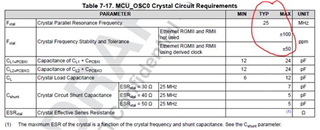
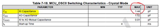
The MCU_OSC0_Xn input has required parameters when using a crystal. (Table 7-17 and Table 7-18)
But we don't specify requirements for an LVCMOS input.
CTRLMMR_MCU_HFOSC0_CTRL (TRM) can be set so we bypass the crystal circuitry.
This allows us to use the LVCMOS digital signal for our clock.
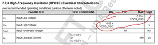
But the section around Figure 7-21 (datasheet) only mentions we need a "1.8V LVCMOS clock source"
What are the requirements?
Frequency: xxMHz ± yy[ppm] what is the required frequency and max variation allowed?
Voltage: V_IH = xx // V_IL = yy what are the max/min input voltage ranges we need to care about in bypass mode?
Duty Cycle: what is the duty cycle requirement of the clock source?
Jitter: what is the jitter requirement (rms or pk-pk) of the clock source?
CL: what is the input capacitance of MCU_OSC0_XI pin in bypass mode?
Tr/Tf: what are the rise/fall time requirements for the clock?
etc...
Can we provide these requirements please?