Other Parts Discussed in Thread: AM2634, ADS7038-Q1, ADS7038
Hi,
for our application we need additional analog input channels besides the one available on the AM2634. Mainly because of different voltage levels in the system an external multichannel ADC with an SPI interface shall be used. Actually the ADS7038-Q1 is our preferred solution. However I am not sure if the chosen solution is the best one, since we do use the called 'On-The-Fly' channel selection mode for the SPI-ADC. To do so we need to issue a transfer every(!) 1.25 usec to write transmit the next channel we want to convert next. Basically it works. However we intend to use the EDMA for many other requests and I am a little un-sure if this system solution will be able to handle all the transfers of data into the on-chip system, despite the fact that this is a multi-core system with a lot of resources and functionality.
Besides the 1.25 us transfers to/from the external SPI-ADC we will need DMA transfers every 5 usec for
- FSI channels
- Data transfers from the Realtime control system to the system memory etc etc
All in all we will need (without any networking DMA) 5..7 channels, two of them every 1.25 usec the remaining channels every 5 usec. Now before I ask the questions I want to show how it shall be done for the external SPI-ADC.
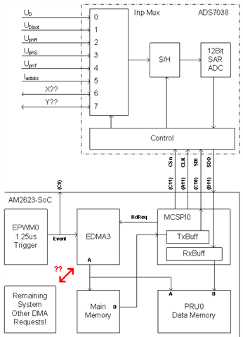
The 'components' on the SoC are shown that are configured to handle the 1.25us transfers. Not shown on the drawing above are the digital isolators needed to isolate the different voltage levels from each other. The AM2634 is on voltage level 'A', the external SPI-ADC is on voltage level 'B'. In real life it looks the following:
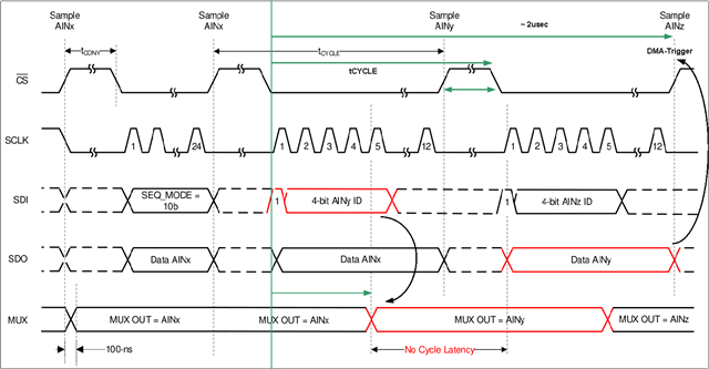
The so called 'On-Thy-Fly' mode of the ADS7038 shall be used in this context. However may be a better approach exists. It looks like each conversion requires the rising edge of the chip select. In other words I can not issue a burst conversion of a bunch of analog input channels with one pin signal event or so ...
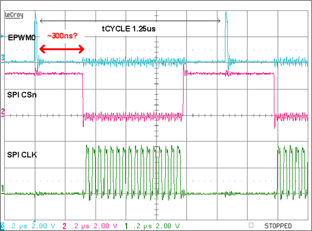
- The 'scope-shot' shows the trigger from the EPWM0 unit every 1.25us (light-blue)
- The chip select from the SPI0 to the external SPI-ADC (Magenta)
- The clock. In this configuration clock speed is 25 MHz, 16 clocks per transfer (Green).
(Not shown on this scope-shot are the data lines SDI and SDO)
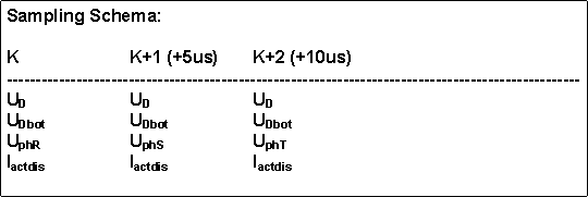
Since more than 4 external channels are needed a sequence with a different order is used to select all the channels needed. After 15 usec this sequence repeats. The table that describes the order of this sequence is in main memory and is read by the DMA. The system shall be configured to run endless. It shall transfer data every 1.25 and 5 usec and process and filter data every 5 usec. On this level of processing is shall operate with mainly 'no-jitter' close as good as it would be if an external FPGA would be used, to guarantee jitter-free operation on this data collection and pre-processing level.
Now the questions (sorry a lot of questions ...):
Q1: Can this be guaranteed with this system approach? I know this question is a little bit ambiguous. However I have no idea how to measure the EDMA3 performance with the involved IP's (MCSPI+RTCS+FSI+PRU) on this system without implementing the whole application which I can't right now. Any idea how I could measure this or make a potential problem visible is very welcome. Please let me know.
Q2: After the EPWM0 event (1.25 us trigger) more than 300ns are needed until the falling edge of the chip select is taking place. How much time is needed for the DMA? Is this mainly because the DMA is 'slow' or is the root-cause the MCSPI-IP configuration? The DMA in this context is reading one-word (16Bit) from the table in the system memory and is writing this one word to the output register/buffer of the MCSPI component in order to select the channel to be converted next. As far as I understand the system clock is 200 MHz for the DMA. Correct?
Q3: Is there a better way to periodically issue a write & data transfer operation as it is done now on the MCSPI0-IP to select and collect the data from the external SPI-ADC? I do use the DMA. I couldn't find any other option for example a timer or an EPWM unit directly. That is the reason why I did use one DMA channel and also because I did use ths 'On-The-Fly' mode of this ADC. However this is not a must.
Q4: Is there a better way to connect an external multi channel ADC to the AM2634 than the MCSPI interface with respect to the system-transfer performance?
Q5: Is it correct that the DMA read request (one data word received from the external SPI-ADC) must be issued after each word? The read request is needed to store the received value into the data memory of the PRU0 for pre-processing. I can not burst-store a packet but must transfer each word? How much time does it take? Or how can I make the time needed visible? As far as I understand there is no option to show the time the DMA is master on the internal system to a GPIO pin for visibility of the occupied bus owner-ship time.
Q6: Is it correct that I can not use DMA and FiFo within the MCSPI at the same time for the same channel? Here I only use channel0 of the MCSPI. I tried to enable and configure the receive Fifo on the MCSPI but doing so I do not get any DMA read requests anymore ...
Hopefully not too many questions. Anyway thanks for sharing and hopefully I can get some ideas to better 'estimate' if the system performance will be enough under all circumstances or if other concepts maybe are better for this type of application.
br
Markus