Part Number: TMS570LS3137
Hi Team,
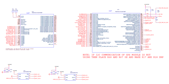
Our customer is using the TMS570LS3137 and would like to know how to configure the ADC connected to pins V8 and V9. Please see attached schematic diagram for reference.

Regards,
Danilo
Part Number: TMS570LS3137
Hi Team,
Our customer is using the TMS570LS3137 and would like to know how to configure the ADC connected to pins V8 and V9. Please see attached schematic diagram for reference.
Regards,
Danilo