Part Number: EK-TM4C123GXL
I've managed to blow up three EK-TM4C123GXL development boards and my stock is running low. I'm applying 5V to various GPIO pins, namely PA2, PA3, PA4, PA5, PA6, PA7, PC4, PC5, PC6, PC7, PD6 and PD7. All the GPIO pins in question are declared 5 V tolerant. (I'm aware that PD4, PD5, PB0 and PB1 are not 5 V tolerant and have avoided these pins.)
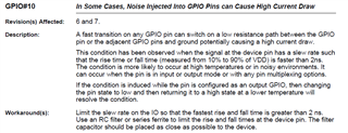
At first I thought, from the "GPIO Pins With Special Considerations" section on p650 of https://www.ti.com/lit/ds/spms376e/spms376e.pdf that perhaps PA2 to PA5 are set as SSI0 functionality at startup. Accordingly I've added the following lines of code to belt-and-braces ensure that all the GPIO pins are set to input:
GPIODirModeSet(GPIO_PORTB_BASE, GPIO_PIN_3, GPIO_DIR_MODE_IN);
GPIOPinTypeGPIOInput(GPIO_PORTB_BASE, GPIO_PIN_3);
GPIOPadConfigSet(GPIO_PORTB_BASE, GPIO_PIN_3, GPIO_STRENGTH_2MA, GPIO_PIN_TYPE_STD_WPD);
The same lines have been applied, with appropriate changes, for all 12 GPIO pins in question.
I wonder if the SSI0 is still in the equation. It's difficult to change over to 3.3V operation, since everything is on a PCB with 5 V in an internal layer, but will do so if there is a known problem with any of the abovementioned 12 pins and 5 V tolerance.
Have I done everything to ensure the pins are inputs? Is there a known problems with any of the listed 12 GPIO pins and 5 V tolerance? Is there a solution to my problem?