This thread has been locked.

If you have a related question, please click the "Ask a related question" button in the top right corner. The newly created question will be automatically linked to this question.

AM2431: GPMC timing specification of CSn and GPMC_AD

Part Number: AM2431


Hi,

I have questions about AM2431 GPMC.
I am planning to use GPMC in Synchronous NOR Flash mode and 32-Bit Address/Data-Multiplexed and GPMCFCLKDIVIDER=0h to communicate with FPGA. And I use GPMC_FCLK_MUX because I want continuous clock output.

Question1: When CSEXTRADELAY=1, is the CSn rising edge timing specification F2 or F3?

Refer to 7.10.5.8.1 GPMC and NOR Flash - Synchronous Mode in the data sheet (www.ti.com/.../am2431), F3 is defined in Table 7-55 as "Delay time, output clock GPMC_CLK rising edge to output chip select GPMC_CSn[i] invalid". F3 is not affected by CSEXTRADELAY=1.

Refer to 12.3.3.5.6.1.2 Synchronous NOR Flash Timing Parameters Formulas in User guide (www.ti.com/.../spruim2), There are descriptions of F related to F2, "For nCS rising edge (chip-select deactivated) in reading mode:" and "For nCS rising edge (chip-select deactivated) in writing mode:". F2 is affected by CSEXTRADELAY=1.

When CSEXTRADELAY=1, Is the CSn rising edge (deactivated or invalid) timing specification F2 or F3?


Question2: When Address/Data Multiplexed, is the first transfer of GPMC_AD the address or the 1st data?

Refer to 7.10.5.8.1 GPMC and NOR Flash - Synchronous Mode in the data sheet (www.ti.com/.../am2431), F15 is defined in Table 7-55 as "Delay time, output clock GPMC_CLK rising edge to output data GPMC_AD[n:0] transition(11)" and "(11) First transfer only for CLK DIV 1 mode".

Does the "first transfer" mean the address or the first data?

best regards,

  • Hi Masanori,

    1. You were referring to a older version of the AM243x datasheet. Please referring to the latest datasheet. It clearly stated that the F2 and F3 are affected by CSEXTRADELAY=1.

    https://www.ti.com/lit/gpn/am2434

    2. The "first transfer" means the address.

    Best regards,

    Ming

  • Hi Ming,
    Thank you for your answers.

    1. I am referring to the latest version of the AM243x datasheet. it revised January 2023.
    F3 is calculated from the value of E.

    CSEXTRADELAY does not affect the value of E.

    Is the expression in E lacking CSEXTRADELAY?

    2. Thanks for the answer.

    Best regards,

    Masanori

  • Hi Masanori,

    Both datasheet and the TRM mentioned the F3 is using F (footnote-6, CSEXTRADELAY is involved) and the F2 is using E (footnot-5, CSEXTRADELAY is not involved), so I think the table -55 is correct.

    Best regards,

    Ming

  • Hi Ming,

    Returning to the first question.
    1. Which timing specification, F2 (deactivated) or F3 (invalid), should a CSn rising edge caused by CSWROFFTIME and CSRDOFFTIME refer to?

    2. In the figure below, if WRDATAONADMUXBUS=2, which timing is D0 output, GPMC_AD (A) or (B)?

    Best regards,
    Masanori

  • Hi Massanori,

    I will forward your questions to our GPMC expert. He will get back to your soon.

    Best regards,

    Ming

  • Hi Massanori,

    Apologies for the delay. We hope to have some replies by the end of the week.

    Regards,
    Mark

  • Hi Massanori, 

    I apologize for the delay on this, I'm taking over the remaining question from Ming. I will reach to the expert once again to bring priority to this, please allow me a until Wednesday to find an acceptable response to the remaining query

    Best,

    Daniel

  • Hi Massanori,

    Sorry about the delay.

    Datasheet Table 7-55 F3 measures when Chip Select is no longer driven by GPMC and returns to its invalid state (high). GPMC only drives CS during an access cycle.
    It uses Access time as the reference point in time because it is required/assumed for synchronous mode that Access Time occurs on a rising edge of GPMC_CLK. The timing F3 measures from rising edge of GPMC_CLK to the end of the cycle when CS is no longer driven (becomes invalid). There is some variability in the output delays from internal GPMC to the signal on the pin. Use this timing to confirm timings on the memory side with regard to CLK and CS.
    One important aspect of note (5) is meant to explain that if a burst is occuring, then the CS will remain active low until the burst completes. It should be updated to include (n - 1) × PageBurstAccessTime like note (2). We will file a LitBug to add this detail.

    F3 is should be a don't care if CSOFFTIME drives CS to a high/OFF state before the end of the cycle. In this case the timing of CS is defined by F2. Note (6) needs to have the rising edge details added like note (7) has for ADV falling edge and ADV rising edge. We will also file a LitBug to add this detail.

    The TRM correctly states in 12.3.3.4.8.1 Read Cycle Time and Write Cycle Time (RDCYCLETIME / WRCYCLETIME)
    When RDCYCLETIME or WRCYCLETIME completes, if they are not already deasserted, all control signals (nCS, nADV/ALE, nOE/RE, nWE, and BE0/CLE) are deasserted to their reset values, regardless of their
    deassertion time parameters.

    Also CSONTIME and CSOFFTIME are explained well in TRM 12.3.3.4.8.2 nCS: Chip-Select Signal Control Assertion/Deassertion Time (CSONTIME / CSRDOFFTIME / CSWROFFTIME / CSEXTRADELAY)

    Regards,
    Mark

  • Hi Mark,

    Thank you for your answer and explanation.
    I understood the definitions of F3 and F2.
    For example, when CSOFFTIME < WRCYCLETIME, CS timing is defined by F2. This includes CSEXTRADELAY.

    I would like you to answer the question about gpmc_ad.
    If WRDATAONADMUXBUS=2, is the timing of address and data output as shown in the diagram below?

    Regards,
    Masanori

  • Hi Manasori,

    our expert is currently out of office, please allow us until the end of the week to answer this remaining question. I apologize for the inconvenience 

    Best,

    Daniel

  • Hi Manasori,

    For example, when CSOFFTIME < WRCYCLETIME, CS timing is defined by F2. This includes CSEXTRADELAY.

    Correct.

    I would like you to answer the question about gpmc_ad.
    If WRDATAONADMUXBUS=2, is the timing of address and data output as shown in the diagram below?

    I think it will be more like the edited figure below.

    "first transfer" means the first data.
    For a burst write with GPMCFCLKDIVIDER = 0 (divide-by-1), the first data is put onto the AD bus on a GPMC_CLK rising edge, but subsequent burst data is put onto the AD bus on a GPMC_CLK falling edge.

    In AD-mux mode, Address will be driven on the AD bus from start of cycle until WRDATAONADMUXBUS # of GPMC_FCLK cycles. For GPMCFCLKDIVIDER = 0 (divide-by-1) this will correspond to a rising GPMC_CLK edge.

    Regards,
    Mark

  • Hi Mark,

    My application uses Address/Data Multiplxed 32-bits(AD-mux) mode and GPMCFCLKDIVIDER=0.
    In AD-mux mode, the data (D0) following the address (A0) is output to the AD bus on a GPMC_CLK rising edge of WRDATAONADMUXBUS# cycles.
    Considering output delay time, is the data(D0) output timing in the following figure correct?

    Regards,
    Masanori

  • Hi Manasori,

    F15 min is a negative value, but in your screenshot it looks like it is positive , slipping to the next positive edge of the GPMC0_CLK. Everything is launched on the internal GPMC_FICLK. The WRDATAONADMUXBUS is not waiting for the external GPMC0_CLK. Instead the transition from address to data occurs on the internal GPMC_FICLK edge. So the transition should occur slightly before or slightly after the blue # 2 CLK edge.

    Best,

    Daniel

  • Hi Daniel,

    F15 specs include J value. J and F15 calculated as follows.

    J = GPMC_FCLK = 15.0 ns.
    F15 min is J -2.3=15.0-2.3=12.7 ns.
    F15 max is J+2.7=15.0+2.7=17.7ns.

    I think the transition should occur slightly before or slightly after the blue # 3 CLK edge.

    Regards,
    Masanori

  • Hi Manasori,

    we need to verify if the min delay shown in the datasheet is actually accurate, so we will be running evaluations in the lab to verify. I appreciate your patience with this, will be back to update by Wednesday.

    Best,

    Daniel

  • Hi Manasori,

    Unfortunately we were not able to capture the data accurately and have to redo our experiment. I will try to get an update on this by today or tomorrow.

    Best,

    Daniel

  • Hi Manasori,

    I apologize for the further delay on this, recently we tried to capture the WRDATAONADMUXBUS timing with GPMC_CLK enabled but ran into issues with the board, we will have to look for a different one, but also our experts are low on bandwidth which further adds to the wait. We will try to find more support on this and update you with an answer by the end of the week. We appreciate your patience a lot.

    Best,

    Daniel

  • Hi Daniel,

    Thank you for trying.
    I look forward to seeing the results.

    Regards,
    Masanori

  • Hi Manasori, 

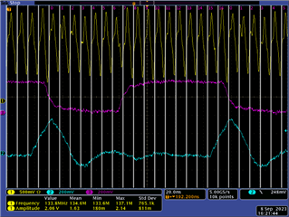
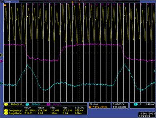
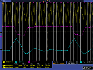
    Below results show that the transition from address to data occurs on the GPMC_FCLK clock cycle set in bit field WRDATAONADMUXBUS.
    The transition does not occur 1 GPMC_FCLK cycle after the GPMC_FCLK edge specified by WRDATAONADMUXBUS as indicated by the datasheet.
    Instead GPMC_FCLK is the reference point, and the signal becomes active on the bus at the specified GPMC_FCLK cycle defined by WRDATAONADMUXBUS -2.3ns to +2.7ns.
    Since GPMC_FCLK cannot be observed directly, you can instead observe GPMC0_CLK with GPMCFCLKDIVIDER = 0 (div-by-1).
    For reference, the address is driven at GPMC_FCLK cycle 0 and the Chip select is driven low at GPMC_FCLK cycle 1.

    WRDATAONADMUXBUS is swept from 7 to 0 in below scope shots

    CH1 (yellow) = GPMC0_CLK
    CH2 (cyan) = GPMC0_CS0n
    CH3 (magenta) = GPMC0_AD12 (every bit on the AD bus transfers from address 0 to data (all F's)

    WRDATAONADMUXBUS = 7

    GPMC_CONFIG1_0  0x28001200
    GPMC_CONFIG2_0  0x00101C01
    GPMC_CONFIG3_0  0x23060917
    GPMC_CONFIG4_0  0x1005BC1A
    GPMC_CONFIG5_0  0x011B111E
    GPMC_CONFIG6_0  0x8F070000
    GPMC_CONFIG7_0  0x00000C50

    =-=-=-=-

    WRDATAONADMUXBUS = 6

    GPMC_CONFIG1_0    0x28001200
    GPMC_CONFIG2_0    0x00101C01
    GPMC_CONFIG3_0    0x23060917
    GPMC_CONFIG4_0    0x1005BC1A
    GPMC_CONFIG5_0    0x011B111E
    GPMC_CONFIG6_0    0x8F060000
    GPMC_CONFIG7_0    0x00000C50

    =-=-=-=-

    WRDATAONADMUXBUS = 5

    GPMC_CONFIG1_0    0x28001200
    GPMC_CONFIG2_0    0x00101C01
    GPMC_CONFIG3_0    0x23060917
    GPMC_CONFIG4_0    0x1005BC1A
    GPMC_CONFIG5_0    0x011B111E
    GPMC_CONFIG6_0    0x8F050000
    GPMC_CONFIG7_0    0x00000C50

    =-=-=-=-

    WRDATAONADMUXBUS = 4

    GPMC_CONFIG1_0    0x28001200
    GPMC_CONFIG2_0    0x00101C01
    GPMC_CONFIG3_0    0x23060917
    GPMC_CONFIG4_0    0x1005BC1A
    GPMC_CONFIG5_0    0x011B111E
    GPMC_CONFIG6_0    0x8F040000
    GPMC_CONFIG7_0    0x00000C50

    =-=-=-=-

    WRDATAONADMUXBUS = 3

    GPMC_CONFIG1_0    0x28001200
    GPMC_CONFIG2_0    0x00101C01
    GPMC_CONFIG3_0    0x23060917
    GPMC_CONFIG4_0    0x1005BC1A
    GPMC_CONFIG5_0    0x011B111E
    GPMC_CONFIG6_0    0x8F030000
    GPMC_CONFIG7_0    0x00000C50

    =-=-=-=-

    WRDATAONADMUXBUS = 2

    GPMC_CONFIG1_0    0x28001200
    GPMC_CONFIG2_0    0x00101C01
    GPMC_CONFIG3_0    0x23060917
    GPMC_CONFIG4_0    0x1005BC1A
    GPMC_CONFIG5_0    0x011B111E
    GPMC_CONFIG6_0    0x8F020000
    GPMC_CONFIG7_0    0x00000C50

    =-=-=-=-

    WRDATAONADMUXBUS = 1

    GPMC_CONFIG1_0    0x28001200
    GPMC_CONFIG2_0    0x00101C01
    GPMC_CONFIG3_0    0x23060917
    GPMC_CONFIG4_0    0x1005BC1A
    GPMC_CONFIG5_0    0x011B111E
    GPMC_CONFIG6_0    0x8F010000
    GPMC_CONFIG7_0    0x00000C50

    =-=-=-=-

    WRDATAONADMUXBUS = 0

    GPMC_CONFIG1_0    0x28001200
    GPMC_CONFIG2_0    0x00101C01
    GPMC_CONFIG3_0    0x23060917
    GPMC_CONFIG4_0    0x1005BC1A
    GPMC_CONFIG5_0    0x011B111E
    GPMC_CONFIG6_0    0x8F000000
    GPMC_CONFIG7_0    0x00000C50

  • Hi Daniel,

    Thank you for the waveform measurement results.
    I understood that when using WRDATAONADMUXBUS, the specification is to set J of F15 to 0.
    The data(D0) output timing is shown in the following figure.

    Regards,
    Masanori