Part Number: AM2634
Other Parts Discussed in Thread: TMDSCNCD263
Hello all,
We have an issue with the XAM2634B controller. We can not program it either via JTAG or via UART.
JTAG verification gives a success state but during connection to the core throws an error. (see gel files output below)
In UART mode the controller resets periodically.
We made a signal level comparison with the TI dev board: TMDSCNCD263 / PROC110E1(001)
Power supplies OK, no glitch (5V, 3v3,1v2,1v8 Pll)
Status of BOOT pins/ Buffer enable signal: OK (verified by oscilloscope and JTAG read back)
Any idea what can cause this issue and what we need to measure or change in CCS to move forward?
Controller's marking on TI dev board: XAM2634B / OLFHMZCZQ / 21ACLSW / G1 / 548 / ZCZ
Controller's marking on User's Board: XAM2634B / OLFHMZCZ / 23CR7PW / G1 / 548 / ZCZ
Thank you very much.
Zoltan
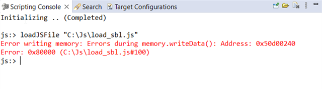
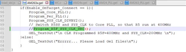
Cortex_R5_0: GEL Output: Loading Gel Files on R5F0
Cortex_R5_0: GEL Output: Gel files loading on R5F0 Complete
Cortex_R5_0: GEL Output: ***OnTargetConnect() Launched***

Cortex_R5_0: GEL Output: AM263x Initialization Scripts Launched.
Please Wait...


Cortex_R5_0: GEL Output: AM263x_Cryst_Clock_Loss_Status() Launched
Cortex_R5_0: GEL Output: Crystal Clock present
Cortex_R5_0: GEL Output: AM263x_SOP_Mode() Launched
Cortex_R5_0: GEL Output: SOP MODE = 0x0000000B
Cortex_R5_0: GEL Output:
 Dev boot mode
Cortex_R5_0: GEL Output: AM263x_Read_Device_Type() Launched
Cortex_R5_0: GEL Output: EFuse Device Type Value = 0x000000AA
Cortex_R5_0: GEL Output: AM263x_Check_supported_mode() Launched
Cortex_R5_0: GEL Output:
 efuse1=0x01000000
Cortex_R5_0: GEL Output:
 The Device supports both LockStep & Dual Core mode
Cortex_R5_0: GEL Output:
 mode = 0
Cortex_R5_0: GEL Output: MSS_CTRL Control Registers Unlocked
Cortex_R5_0: GEL Output: MSS_TOP_RCM Control Registers Unlocked
Cortex_R5_0: GEL Output: MSS_RCM Control Registers Unlocked
Cortex_R5_0: GEL Output: MSS_IOMUX Control Registers Unlocked
Cortex_R5_0: GEL Output: TOP_CTRL Control Registers Unlocked
Cortex_R5_0: GEL Output:

***R5FSS0 Reset for Lockstep ***
Cortex_R5_0: GEL Output:

*** R5FSS1 Reset for Lockstep ***
Cortex_R5_0: GEL Output: R5F ROM Eclipse
Cortex_R5_0: GEL Output: R5FSS0_0 Released
Cortex_R5_0: GEL Output: R5FSS0_1 Released
Cortex_R5_0: GEL Output: R5FSS1_0 Released
Cortex_R5_0: GEL Output: R5FSS1_1 Released
Cortex_R5_0: GEL Output:

 All R5F Cores Released for program load
Cortex_R5_0: GEL Output: L2 Mem Init Complete
Cortex_R5_0: GEL Output: MailBox Mem Init Complete
Cortex_R5_0: GEL Output: *********** R5FSS0/1 Lockstep mode Configured********
Cortex_R5_0: GEL Output: CORE PLL Configuration Complete
Cortex_R5_0: GEL Output: PER PLL Configuration Complete
Cortex_R5_0: GEL Output: SYS_CLK DIVBY2
Cortex_R5_0: Trouble Writing Memory Block at 0x53200500 on Page 0 of Length 0x4: (Error -1170 @ 0x53200504) Unable to access the DAP. Reset the device, and retry the operation. If error persists, confirm configuration, power-cycle the board, and/or try more reliable JTAG settings (e.g. lower TCLK). (Emulation package 9.11.0.00128)
Cortex_R5_0: GEL: Error while executing OnTargetConnect(): Target failed to write 0x53200500
	 at *(p_mmr)=mmr_value [AM263_common.gel:287]
	 at Write_MMR((0x53200000U+0x00000500U), src_sel_val) [AM263_PLL.gel:284]
	 at Program_R5F_SYS_CLK_SRC() [AM263x.gel:206]
	 at Configure_Plls_R5F_400_SYS_200_Clocks() [AM263x.gel:124]
	 at OnTargetConnect()
Cortex_R5_0: GEL Output: ***OnTargetConnect() Launched***

Cortex_R5_0: GEL Output: AM263x Initialization Scripts Launched.
Please Wait...


Cortex_R5_0: GEL Output: AM263x_Cryst_Clock_Loss_Status() Launched
Cortex_R5_0: GEL Output: Crystal Clock present
Cortex_R5_0: GEL Output: AM263x_SOP_Mode() Launched
Cortex_R5_0: GEL Output: SOP MODE = 0x0000000B
Cortex_R5_0: GEL Output:
 Dev boot mode
Cortex_R5_0: GEL Output: AM263x_Read_Device_Type() Launched
Cortex_R5_0: GEL Output: EFuse Device Type Value = 0x000000AA
Cortex_R5_0: GEL Output: AM263x_Check_supported_mode() Launched
Cortex_R5_0: GEL Output:
 efuse1=0x01000000
Cortex_R5_0: GEL Output:
 The Device supports both LockStep & Dual Core mode
Cortex_R5_0: GEL Output:
 mode = 0
Cortex_R5_0: GEL Output: MSS_CTRL Control Registers Unlocked
Cortex_R5_0: GEL Output: MSS_TOP_RCM Control Registers Unlocked
Cortex_R5_0: GEL Output: MSS_RCM Control Registers Unlocked
Cortex_R5_0: GEL Output: MSS_IOMUX Control Registers Unlocked
Cortex_R5_0: GEL Output: TOP_CTRL Control Registers Unlocked
Cortex_R5_0: GEL Output:

***R5FSS0 Reset for Lockstep ***
Cortex_R5_0: GEL Output:

*** R5FSS1 Reset for Lockstep ***
Cortex_R5_0: GEL Output: R5F ROM Eclipse
Cortex_R5_0: GEL Output: R5FSS0_0 Released
Cortex_R5_0: GEL Output: R5FSS0_1 Released
Cortex_R5_0: GEL Output: R5FSS1_0 Released
Cortex_R5_0: GEL Output: R5FSS1_1 Released
Cortex_R5_0: GEL Output:

 All R5F Cores Released for program load
Cortex_R5_0: GEL Output: L2 Mem Init Complete
Cortex_R5_0: GEL Output: MailBox Mem Init Complete
Cortex_R5_0: GEL Output: *********** R5FSS0/1 Lockstep mode Configured********
Cortex_R5_0: GEL Output: CORE PLL Configuration Complete
Cortex_R5_0: GEL Output: PER PLL Configuration Complete
Cortex_R5_0: GEL Output: SYS_CLK DIVBY2
Cortex_R5_0: GEL Output: DPLL_CORE_HSDIV0_CLKOUT0 selected as CLK source for R5FSS & SYS CLKs
Cortex_R5_0: GEL Output:
 CLK Programmed R5F=400MHz and SYS_CLK=200MHz
Cortex_R5_0: GEL Output:

 *** Enabling Peripheral Clocks ***
Cortex_R5_0: GEL Output: Enabling RTI[0:3] Clocks
Cortex_R5_0: GEL Output: Enabling RTI_WDT[0:3] Clocks
Cortex_R5_0: GEL Output: Enabling UART[0:5]/LIN[0:5] Clocks
Cortex_R5_0: GEL Output: Enabling QSPI Clocks
Cortex_R5_0: GEL Output: Enabling I2C Clocks
Cortex_R5_0: GEL Output: Enabling TRACE Clocks
Cortex_R5_0: GEL Output: Enabling MCAN[0:3] Clocks
Cortex_R5_0: GEL Output: Enabling GPMC Clocks
Cortex_R5_0: GEL Output: Enabling ELM Clocks
Cortex_R5_0: GEL Output: Enabling MMCSD Clocks
Cortex_R5_0: GEL Output: Enabling MCSPI[0:4] Clocks
Cortex_R5_0: GEL Output: Enabling CONTROLSS Clocks
Cortex_R5_0: GEL Output: Enabling CPTS Clocks
Cortex_R5_0: GEL Output: Enabling RGMI[5,50,250] Clocks
Cortex_R5_0: GEL Output: Enabling XTAL_TEMPSENSE_32K Clocks
Cortex_R5_0: GEL Output: Enabling XTAL_MMC_32K Clocks
Cortex_R5_0: GEL Output:

 ***All IP Clocks are Enabled***
[Start]

Execute the command:

%ccs_base%/common/uscif/dbgjtag -f %boarddatafile% -rv -o -S integrity

[Result]


-----[Print the board config pathname(s)]------------------------------------

C:\Users\RNDEEN~1\AppData\Local\TEXASI~1\
    CCS\ccs1220\0\0\BrdDat\testBoard.dat

-----[Print the reset-command software log-file]-----------------------------

This utility has selected a 100/110/510 class product.
This utility will load the adapter 'jioxds110.dll'.
The library build date was 'Mar 10 2023'.
The library build time was '17:27:27'.
The library package version is '9.11.0.00128'.
The library component version is '35.35.0.0'.
The controller does not use a programmable FPGA.
The controller has a version number of '5' (0x00000005).
The controller has an insertion length of '0' (0x00000000).
This utility will attempt to reset the controller.
This utility has successfully reset the controller.

-----[Print the reset-command hardware log-file]-----------------------------

The scan-path will be reset by toggling the JTAG TRST signal.
The controller is the XDS110 with USB interface.
The link from controller to target is direct (without cable).
The software is configured for XDS110 features.
The controller cannot monitor the value on the EMU[0] pin.
The controller cannot monitor the value on the EMU[1] pin.
The controller cannot control the timing on output pins.
The controller cannot control the timing on input pins.
The scan-path link-delay has been set to exactly '0' (0x0000).

-----[Perform the Integrity scan-test on the JTAG IR]------------------------

This test will use blocks of 64 32-bit words.
This test will be applied just once.

Do a test using 0xFFFFFFFF.
Scan tests: 1, skipped: 0, failed: 0
Do a test using 0x00000000.
Scan tests: 2, skipped: 0, failed: 0
Do a test using 0xFE03E0E2.
Scan tests: 3, skipped: 0, failed: 0
Do a test using 0x01FC1F1D.
Scan tests: 4, skipped: 0, failed: 0
Do a test using 0x5533CCAA.
Scan tests: 5, skipped: 0, failed: 0
Do a test using 0xAACC3355.
Scan tests: 6, skipped: 0, failed: 0
All of the values were scanned correctly.

The JTAG IR Integrity scan-test has succeeded.

-----[Perform the Integrity scan-test on the JTAG DR]------------------------

This test will use blocks of 64 32-bit words.
This test will be applied just once.

Do a test using 0xFFFFFFFF.
Scan tests: 1, skipped: 0, failed: 0
Do a test using 0x00000000.
Scan tests: 2, skipped: 0, failed: 0
Do a test using 0xFE03E0E2.
Scan tests: 3, skipped: 0, failed: 0
Do a test using 0x01FC1F1D.
Scan tests: 4, skipped: 0, failed: 0
Do a test using 0x5533CCAA.
Scan tests: 5, skipped: 0, failed: 0
Do a test using 0xAACC3355.
Scan tests: 6, skipped: 0, failed: 0
All of the values were scanned correctly.

The JTAG DR Integrity scan-test has succeeded.

[End]