Hello,
I'm trying to get to grips with the TCM concept but it is being made difficult by a disparity between the TRM and the register database file AM263x.xml for register and bitfield names.
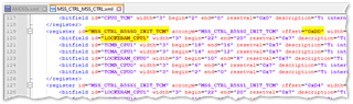
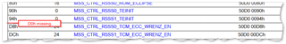
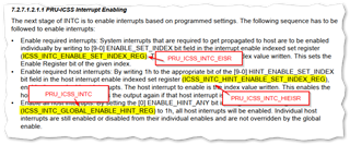
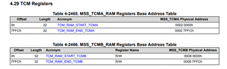
None of the following highlighted items can be found in the database if they are taken at face value:
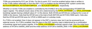
I managed to find one of them after some head scratching. CPUn_LOCZRAMA in the manual is actually LOCKZRAM_CPUn in the database. Is that correct?