This thread has been locked.

If you have a related question, please click the "Ask a related question" button in the top right corner. The newly created question will be automatically linked to this question.

TM4C123GH6PM: Help integrating flash bootloader into application project

Part Number: TM4C123GH6PM

Hello,

I'm trying to import the flash bootloader into my application project.  I've located a very helpful example project with the help of a TI forum support engineer (Charles).  I'm trying to figure out how to tell the tool (CCS compiler/linker - I think mainly the linker?) where to place the flash bootloader vs the application project.  I've been looking at the project settings for the boot_serial example for the TM4C123GXL board project and see the bl_link_ccs.cmd has an "init_load" for LOAD_START and a "init_run" for RUN_START.

To bring the boot_serial source code / boot loader into my application what exactly do I need to configure so that the bootloader is placed at 0x00000000 and my application is placed at 0x00002800?  A comparison of the .cmd files shows that the boot_serial *.cmd file has two separate groups where my *.cmd file does not.  

Below are the two .cmd files - one from boot_serial example and one from my application project:

boot_serial exmaple

MEMORY
{
    FLASH (RX) : origin = 0x00000000, length = 0x00010000
    SRAM (RWX) : origin = 0x20000000, length = 0x00010000
}

/* Section allocation in memory */

SECTIONS
{
    GROUP
    {
        .intvecs
        .text
        .const
        .data
    } load = FLASH, run = 0x20000000, LOAD_START(init_load), RUN_START(init_run), SIZE(init_size)

    GROUP
    {
        .bss
        .stack
    } run = SRAM, RUN_START(bss_run), RUN_END(bss_end), SIZE(bss_size), RUN_END(__STACK_TOP)

}

Current application project

#define APP_BASE 0x00000000
#define RAM_BASE 0x20000000

/* System memory map */

MEMORY
{
    /* Application stored in and executes from internal flash */
    FLASH (RX) : origin = APP_BASE, length = 0x00040000
    /* Application uses internal RAM for data */
    SRAM (RWX) : origin = 0x20000000, length = 0x00008000
}

/* Section allocation in memory */

SECTIONS
{
    .intvecs:   > APP_BASE
    .text   :   > FLASH
    .const  :   > FLASH
    .cinit  :   > FLASH
    .pinit  :   > FLASH
    .init_array : > FLASH

    .vtable :   > RAM_BASE
    .data   :   > SRAM
    .bss    :   > SRAM
    .sysmem :   > SRAM
    .stack  :   > SRAM
#ifdef  __TI_COMPILER_VERSION__
#if     __TI_COMPILER_VERSION__ >= 15009000
    .TI.ramfunc : {} load=FLASH, run=SRAM, table(BINIT)
#endif
#endif
}

__STACK_TOP = __stack + 1024;

I'm also wondering if I need to edit the .cmd file or do I need to use the project properties (right click on project in CCS and select properties) to set this information?

Thanks

  • Forgot to post the block diagram of what I'm trying to accomplish so see below in case this is helpful.

  • Hi Robert,

    To bring the boot_serial source code / boot loader into my application what exactly do I need to configure so that the bootloader is placed at 0x00000000 and my application is placed at 0x00002800?

    For your application, the APP_BASE needs to be 0x2800. However, reading your application linker file, it shows that you have APP_BASE equal to 0x00000000 like below. Please change it to 0x2800. 

    #define APP_BASE 0x00000000

    You can reference the boot_demo1 example. This is the application example that is used in conjunction with boot_serial. Below is the linker command file where you see that APP_BASE is defined as 0x2800. 

    --retain=g_pfnVectors
    
    /* The following command line options are set as part of the CCS project.    */
    /* If you are building using the command line, or for some reason want to    */
    /* define them here, you can uncomment and modify these lines as needed.     */
    /* If you are using CCS for building, it is probably better to make any such */
    /* modifications in your CCS project and leave this file alone.              */
    /*                                                                           */
    /* --heap_size=0                                                             */
    /* --stack_size=256                                                          */
    /* --library=rtsv7M3_T_le_eabi.lib                                           */
    
    /* The starting address of the application.  Normally the interrupt vectors  */
    /* must be located at the beginning of the application.                      */
    #define APP_BASE 0x00002800
    #define RAM_BASE 0x20000000
    
    /* System memory map */
    
    MEMORY
    {
        /* Application stored in and executes from internal flash */
        FLASH (RX) : origin = APP_BASE, length = 0x0003d800
        /* Application uses internal RAM for data */
        SRAM (RWX) : origin = 0x20000000, length = 0x00008000
    }
    
    /* Section allocation in memory */
    
    SECTIONS
    {
        .intvecs:   > APP_BASE
        .text   :   > FLASH
        .const  :   > FLASH
        .cinit  :   > FLASH
        .pinit  :   > FLASH
        .init_array : > FLASH
    
        .vtable :   > RAM_BASE
        .data   :   > SRAM
        .bss    :   > SRAM
        .sysmem :   > SRAM
        .stack  :   > SRAM
    #ifdef  __TI_COMPILER_VERSION__
    #if     __TI_COMPILER_VERSION__ >= 15009000
        .TI.ramfunc : {} load=FLASH, run=SRAM, table(BINIT)
    #endif
    #endif
    }
    
    __STACK_TOP = __stack + 1024;

  • Hi Charles,

    So following the example was helpful.  I think I had a fundamental misunderstanding about how to do this.  Let me know your thoughts on the following questions:

    1. Is it correct to take the approach of having the flash bootloader as a completely separate project?  You program the flash bootloader project first at address 0x00000000.  Once done you program your "application project" which is a completely separate project as a second programming operation?

    2. In bl_config.h what is RCGCGPIO_Rx referring to?  This is shown below and found on line #1169

    //*****************************************************************************
    //
    // Specifies the GPIO peripheral containing the pin which is used for DP.
    // The value is of the form SYSCTL_RCGCGPIO_Rx, where the Rx represents
    // the required GPIO port.  This applies to Blizzard class and later 
    // devices.
    //
    // Depends on: USB_ENABLE_UPDATE, USB_DP_CONFIG
    // Exclusive of: None
    // Requires: None
    //
    //*****************************************************************************
    //#define USB_DP_PERIPH          SYSCTL_RCGCGPIO_R10            // For EK-TM4C1294XL
    #define USB_DP_PERIPH          SYSCTL_RCGCGPIO_R3            // For EK-TM4C123GXL

    3. Is the expectation to only change my linker #define APP_BASE value as shown below?  When trying this my application just crashes.  Screenshot shown below from CCS.  I'm worried there are more settings to modify to support this that I'm missing.  

    /******************************************************************************
     *
     * usb_dev_bulk_ccs.cmd - CCS linker configuration file for usb_dev_bulk.
     *
     * Copyright (c) 2012-2020 Texas Instruments Incorporated.  All rights reserved.
     * Software License Agreement
     * 
     * Texas Instruments (TI) is supplying this software for use solely and
     * exclusively on TI's microcontroller products. The software is owned by
     * TI and/or its suppliers, and is protected under applicable copyright
     * laws. You may not combine this software with "viral" open-source
     * software in order to form a larger program.
     * 
     * THIS SOFTWARE IS PROVIDED "AS IS" AND WITH ALL FAULTS.
     * NO WARRANTIES, WHETHER EXPRESS, IMPLIED OR STATUTORY, INCLUDING, BUT
     * NOT LIMITED TO, IMPLIED WARRANTIES OF MERCHANTABILITY AND FITNESS FOR
     * A PARTICULAR PURPOSE APPLY TO THIS SOFTWARE. TI SHALL NOT, UNDER ANY
     * CIRCUMSTANCES, BE LIABLE FOR SPECIAL, INCIDENTAL, OR CONSEQUENTIAL
     * DAMAGES, FOR ANY REASON WHATSOEVER.
     * 
     * This is part of revision 2.2.0.295 of the EK-TM4C123GXL Firmware Package.
     *
     *****************************************************************************/
    
    --retain=g_pfnVectors
    
    /* The following command line options are set as part of the CCS project.    */
    /* If you are building using the command line, or for some reason want to    */
    /* define them here, you can uncomment and modify these lines as needed.     */
    /* If you are using CCS for building, it is probably better to make any such */
    /* modifications in your CCS project and leave this file alone.              */
    /*                                                                           */
    /* --heap_size=0                                                             */
    /* --stack_size=256                                                          */
    /* --library=rtsv7M3_T_le_eabi.lib                                           */
    
    /* The starting address of the application.  Normally the interrupt vectors  */
    /* must be located at the beginning of the application.                      */
    //#define APP_BASE 0x00000000
    #define APP_BASE 0x00002800
    #define RAM_BASE 0x20000000
    
    /* System memory map */
    
    MEMORY
    {
        /* Application stored in and executes from internal flash */
        FLASH (RX) : origin = APP_BASE, length = 0x00040000
        /* Application uses internal RAM for data */
        SRAM (RWX) : origin = 0x20000000, length = 0x00008000
    }
    
    /* Section allocation in memory */
    
    SECTIONS
    {
        .intvecs:   > APP_BASE
        .text   :   > FLASH
        .const  :   > FLASH
        .cinit  :   > FLASH
        .pinit  :   > FLASH
        .init_array : > FLASH
    
        .vtable :   > RAM_BASE
        .data   :   > SRAM
        .bss    :   > SRAM
        .sysmem :   > SRAM
        .stack  :   > SRAM
    #ifdef  __TI_COMPILER_VERSION__
    #if     __TI_COMPILER_VERSION__ >= 15009000
        .TI.ramfunc : {} load=FLASH, run=SRAM, table(BINIT)
    #endif
    #endif
    }
    
    __STACK_TOP = __stack + 1024;

    4. Does the debug session need to be updated so it knows to run the application project from 0x2800?  I'm wondering if my issue in #3 is due to this.  I've looked around today but didn't find a field specifying where the debugger should start running code? I wonder if you need to change from address 0 no to 0x2800.

    Thanks

  • 1. Is it correct to take the approach of having the flash bootloader as a completely separate project?  You program the flash bootloader project first at address 0x00000000.  Once done you program your "application project" which is a completely separate project as a second programming operation?

    Hi Robert,

      Yes, the flash bootloader is a completely separate project residing at 0x0.  It is a small piece of program that you will first use JTAG to load it. Once the bootloader is running, it will download your application firmware (e.g. boot_demo1.c) from your specified communication port (.e.g. UART). Since the flash bootloader resides at 0x0, you cannot have the firmware also residing at 0x0. It needs to be somewhere else such as 0x2800 or an address offset that is a multiple of 1024 bytes. 

    2. In bl_config.h what is RCGCGPIO_Rx referring to?  This is shown below and found on line #1169

    Fullscreen
    1
    2
    3
    4
    5
    6
    7
    8
    9
    10
    11
    12
    13
    14
    //*****************************************************************************
    //
    // Specifies the GPIO peripheral containing the pin which is used for DP.
    // The value is of the form SYSCTL_RCGCGPIO_Rx, where the Rx represents
    // the required GPIO port. This applies to Blizzard class and later
    // devices.
    //
    // Depends on: USB_ENABLE_UPDATE, USB_DP_CONFIG
    // Exclusive of: None
    // Requires: None
    //
    //*****************************************************************************
    //#define USB_DP_PERIPH SYSCTL_RCGCGPIO_R10 // For EK-TM4C1294XL
    #define USB_DP_PERIPH SYSCTL_RCGCGPIO_R3 // For EK-TM4C123GXL
    XXXXXXXXXXXXXXXXXXXXXXXXXXXXXXXXXXXXXXXXXXXXXXXXXX

    3

    Here, as you know the USB DP pin is mapped to PD5. You would need to configure the bootloader to first enable PortD. This is what the line bl_config.h is doing. It is also configuring for other USB pins like DM, VBUS and ID. 

    3. Is the expectation to only change my linker #define APP_BASE value as shown below?  When trying this my application just crashes.  Screenshot shown below from CCS.  I'm worried there are more settings to modify to support this that I'm missing.  

    Yes, when you build your application firmware you will need to allocate the firmware to start at 0x02800 by changing APP_BASE to 0x2800. This address must match the bootloader APP_START_ADDRESS and VTABLE_START_ADDRESS in the bl_config.h file. 

    //*****************************************************************************
    //
    // The starting address of the application. This must be a multiple of 1024
    // bytes (making it aligned to a page boundary). A vector table is expected at
    // this location, and the perceived validity of the vector table (stack located
    // in SRAM, reset vector located in flash) is used as an indication of the
    // validity of the application image.
    //
    // The flash image of the boot loader must not be larger than this value.
    //
    // Depends on: None
    // Exclusive of: None
    // Requires: None
    //
    //*****************************************************************************
    #define APP_START_ADDRESS 0x2800

    //*****************************************************************************
    //
    // The address at which the application locates its exception vector table.
    // This must be a multiple of 1024 bytes (making it aligned to a page
    // boundary). Typically, an application will start with its vector table and
    // this value should be set to APP_START_ADDRESS. This option is provided to
    // cater for applications which run from external memory which may not be
    // accessible by the NVIC (the vector table offset register is only 30 bits
    // long).
    //
    // Depends on: None
    // Exclusive of: None
    // Requires: None
    //
    //*****************************************************************************
    #define VTABLE_START_ADDRESS 0x2800

    4. Does the debug session need to be updated so it knows to run the application project from 0x2800?  I'm wondering if my issue in #3 is due to this.  I've looked around today but didn't find a field specifying where the debugger should start running code? I wonder if you need to change from address 0 no to 0x2800.

    After the flash bootloader is running, it will download your firmware from your specified interface (e.g. UART, USB, CAN, SPI or I2C) if there is nothing residing at 0x2800. If it finds that there is already valid stack pointer and reset vector at 0x2800 then the bootloader will simply just jump to 0x2800 to run the application. After reset cycle, the processor starts at 0x0 which is running the bootloader. The bootloader decides if it needs to jump to the application or not. There is nothing to configure for the debugger to know where the application is. 

    I will suggest you play with the boot_serial (the bootloader) and the boot_demo1 (the application) as is. Get a feel for how it works using UART. 

  • Hi Charles,

    So I think I've finally found the root cause of my issue.  It looks like there is an "instruction access violation" BIT 0 in register HFAULTSTAT that happens when I change the #define APP_BASE from 0 to 0x02800.  I initially thought this was a bootloading problem.

    I'll be troubleshooting this now as my problem is due to a fault that happens because I change my APP_BASE.  I'll attach the fault info in case you happen to have run into this before.  My PC register becomes 0xFFFFFFFE and my LR becomes 0xFFFFFFF1 which I'm not too sure what to make of yet.  My stack pointer points to a value in the middle of my 1024 byte stack and shows an address of 0x200032F0.

    It seems as though changing APP_BASE does affect something else as this project works fine when APP_BASE = 0, but not when 0x02800.  

  • Hi Robert,

      Was the application successfully loaded by the bootloader via the USB interface?

      Is the fault problem you are seeing happens after the bootloader jumps to the application or the problem happens after the application jumps back to the bootloader?

      Can you use the memory browser to view the content of the flash at 0x0 and 0x2800? Is the bootloader still there at 0x0? Is the application loaded at 0x2800?

  • Hi Charles,

    So I think this issue is unrelated to the bootloader.  My first step was to take my working application project and just change APP_BASE to verify it still works and it seems that changing APP_BASE breaks the project.  So I haven't gotten to the bootloader part yet.  The steps I took are as follows:

    1. Change APP_BASE to 0x2800 in my working application project.  Shown in code view below.

    /* The starting address of the application.  Normally the interrupt vectors  */
    /* must be located at the beginning of the application.                      */
    //#define APP_BASE 0x00000000
    #define APP_BASE 0x00002800
    #define RAM_BASE 0x20000000
    
    /* System memory map */
    
    MEMORY
    {
        /* Application stored in and executes from internal flash */
        FLASH (RX) : origin = APP_BASE, length = 0x00040000
        /* Application uses internal RAM for data */
        SRAM (RWX) : origin = 0x20000000, length = 0x00008000
    }
    
    /* Section allocation in memory */
    
    SECTIONS
    {
        .intvecs:   > APP_BASE
        .text   :   > FLASH
        .const  :   > FLASH
        .cinit  :   > FLASH
        .pinit  :   > FLASH
        .init_array : > FLASH
    
        .vtable :   > RAM_BASE
        .data   :   > SRAM
        .bss    :   > SRAM
        .sysmem :   > SRAM
        .stack  :   > SRAM
    #ifdef  __TI_COMPILER_VERSION__
    #if     __TI_COMPILER_VERSION__ >= 15009000
        .TI.ramfunc : {} load=FLASH, run=SRAM, table(BINIT)
    #endif
    #endif
    }
    
    __STACK_TOP = __stack + 1024;
    

    2. Next I clean and build my project.

    3. Program using debugger in CCS to test application on launchpad to verify it still works.

    4. Once CCS enters debugger mode I just click "run" then "pause" and I see that "instruction access violation".

    So per your questions - I'm currently just trying to get my application project to run with the new APP_BASE.  I do see the bootloader gong to address 0 when I program it, but right now I'm not even doing that. I'm only trying to get my application to work properly with the new APP_BASE value.  

    The application project is getting loaded at the correct address I think.  Below is a screenshot of the memory view at 0x2800 which I believe shows the interrupt pointer function table for my application which makes sense.

    I can see main just after this

    So it looks like the application is being placed correctly, but during operation I run into this instruction fault.  I also think this fault is due to an interrupt because I can run some of the application code in the debugger, but when APP_BASE = 0x2800 I never hit my breakpoint in my SysTick interrupt handler.  When I set APP_BASE = 0 everything works fine.

    This issue is difficult to troubleshoot because my link register LR doesn't have the exit code address as you can see.  So I can't figure out what the calling function was before this crash.

    So does that make more sense?  I don't think this has anything to do with boot loader code, just a bug due to changing APP_BASE = 0x2800.

    Thanks

  • Hi Robert,

      What you are doing will not work. If you just load your application using JTAG with the application allocated to 0x2800 then there is nothing at 0x0. It is possible that you first load the bootloader using JTAG and later load the application using JTAG again. If you load the application using JTAG in CCS, it will erase the flash at 0x0. This is why I ask you to show the content of flash at 0x0. If you see all F's then there is no bootloader at 0x0. When processor comes out of reset, it starts at 0x0 looking for a valid stack pointer and a valid reset vector at 0x4. If they are all 0xF then you will get a fault. 

      Try to use Uniflash which can load multiple images at the same time. You would load the bootloader image starting at 0x0 and the application image at 0x2800 at the same time by specifying both binary files. Uniflash can do this easily. You can't use CCS to load multiple images at the same time but there is a trick to workaround it. You would first load the bootloader image. But before you load the application image, you need to instruct CCS programmer not to erase the first flash sector for which the bootloader resides. By default, a load program will first erase the flash completely before programming the code. 

  • Ok - that was my original plan.  I loaded the bootloader and then configured my application project to only erase flash from 0x2800-0x3FFFF.  This now seems to work until I enable interrupts.  The CPU tries to jump to instruction at 0x528 and crashes out.  I need to look at this more, but it seems as though everything works until I enable interrupts now.  There must be something wrong with the interrupt table.  

    The last thing I do in my main function configuration is "IntMasterEnable();" and once this executes I crash out with address 0x538 which shouldn't ever happen because that is in the bootloader space.  There is some bug where the CPU is jumping to code in the bootloader section when an interrupt fires.

    Hopefully this is easier to debug now that I have useful information in the core registers.

  • Hey Charles,

    So it looks like after some work this weekend the CPU fault was due to the project settings - specifically not resetting the MCU on program load or restart.  Once I checked this box in my application project debug settings I am now able to load both the bootloader and my application project successfully.  So a little bit of a curve ball due to project settings.  I guess there was some old register settings somewhere not being reset when I was loading my application project.

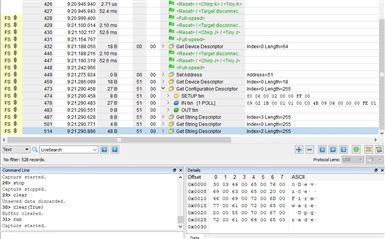
    With this issue solved, I'm back to trying to get the flash bootloader working with USB.  With the following settings I don't see the device enumerate correctly.  Do you see anything wrong with my bl_config.h file?  

    I've followed your advice and used the "boot_serial" application and attempted to change it over to be a usb bootloader instead of serial.  I think I am close however the bootloader doesn't fully enumerate as a DFU device.  It seems to get stuck.  My guess is there is a configuration problem, but I'm not seeing it.  

    Also, should my bootloader launch code look like the boot_demo2 project - code shown below?  I ask because when I use this it doesn't work - unless there is an issue with bl_config.h.  I guess that could be causing this issue too.

    //*****************************************************************************
    //
    // Passes control to the boot loader and initiates a remote software update.
    //
    // This function passes control to the boot loader and initiates an update of
    // the main application firmware image via UART0, Ethernet or USB depending
    // upon the specific boot loader binary in use.
    //
    //*****************************************************************************
    void
    JumpToBootLoader(void)
    {
        //
        // We must make sure we turn off SysTick and its interrupt before entering 
        // the boot loader!
        //
        ROM_SysTickIntDisable(); 
        ROM_SysTickDisable(); 
    
        //
        // Disable all processor interrupts.  Instead of disabling them
        // one at a time, a direct write to NVIC is done to disable all
        // peripheral interrupts.
        //
        HWREG(NVIC_DIS0) = 0xffffffff;
        HWREG(NVIC_DIS1) = 0xffffffff;
    
        //
        // Return control to the boot loader.  This is a call to the SVC
        // handler in the boot loader.
        //
        (*((void (*)(void))(*(uint32_t *)0x2c)))(); 
    }

    What usb flash bootloader looks like in device manager:

    bl_config.h is shown below - I couldn't find a way to attach a file.  I apologize for how long this is.  Let me know if there is an "attach file" option on these forums.

    //*****************************************************************************
    //
    // bl_config.h - The configurable parameters of the boot loader.
    //
    // Copyright (c) 2012-2020 Texas Instruments Incorporated.  All rights reserved.
    // Software License Agreement
    // 
    // Texas Instruments (TI) is supplying this software for use solely and
    // exclusively on TI's microcontroller products. The software is owned by
    // TI and/or its suppliers, and is protected under applicable copyright
    // laws. You may not combine this software with "viral" open-source
    // software in order to form a larger program.
    // 
    // THIS SOFTWARE IS PROVIDED "AS IS" AND WITH ALL FAULTS.
    // NO WARRANTIES, WHETHER EXPRESS, IMPLIED OR STATUTORY, INCLUDING, BUT
    // NOT LIMITED TO, IMPLIED WARRANTIES OF MERCHANTABILITY AND FITNESS FOR
    // A PARTICULAR PURPOSE APPLY TO THIS SOFTWARE. TI SHALL NOT, UNDER ANY
    // CIRCUMSTANCES, BE LIABLE FOR SPECIAL, INCIDENTAL, OR CONSEQUENTIAL
    // DAMAGES, FOR ANY REASON WHATSOEVER.
    // 
    // This is part of revision 2.2.0.295 of the EK-TM4C123GXL Firmware Package.
    //
    //*****************************************************************************
    
    #ifndef __BL_CONFIG_H__
    #define __BL_CONFIG_H__
    
    //*****************************************************************************
    //
    // The following defines are used to configure the operation of the boot
    // loader.  For each define, its interactions with other defines are described.
    // First is the dependencies (in other words, the defines that must also be
    // defined if it is defined), next are the exclusives (in other words, the
    // defines that can not be defined if it is defined), and finally are the
    // requirements (in other words, the defines that must be defined if it is
    // defined).
    //
    // The following defines must be defined in order for the boot loader to
    // operate:
    //
    //     One of CAN_ENABLE_UPDATE, ENET_ENABLE_UPDATE, I2C_ENABLE_UPDATE,
    //            SSI_ENABLE_UPDATE, UART_ENABLE_UPDATE, or USB_ENABLE_UPDATE
    //     APP_START_ADDRESS
    //     VTABLE_START_ADDRESS
    //     FLASH_PAGE_SIZE
    //     STACK_SIZE
    //
    //*****************************************************************************
    
    //*****************************************************************************
    //
    // The frequency of the crystal used to clock the microcontroller.
    //
    // This defines the crystal frequency used by the microcontroller running the
    // boot loader.  If this is unknown at the time of production, then use the
    // UART_AUTOBAUD feature to properly configure the UART.
    //
    // Depends on: None
    // Exclusive of: None
    // Requires: None
    //
    //*****************************************************************************
    #define CRYSTAL_FREQ            16000000
    
    //*****************************************************************************
    //
    // The starting address of the application.  This must be a multiple of 1024
    // bytes (making it aligned to a page boundary).  A vector table is expected at
    // this location, and the perceived validity of the vector table (stack located
    // in SRAM, reset vector located in flash) is used as an indication of the
    // validity of the application image.
    //
    // The flash image of the boot loader must not be larger than this value.
    //
    // Depends on: None
    // Exclusive of: None
    // Requires: None
    //
    //*****************************************************************************
    #define APP_START_ADDRESS       0x2800
    
    //*****************************************************************************
    //
    // The address at which the application locates its exception vector table.
    // This must be a multiple of 1024 bytes (making it aligned to a page
    // boundary).  Typically, an application will start with its vector table and
    // this value should be set to APP_START_ADDRESS.  This option is provided to
    // cater for applications which run from external memory which may not be
    // accessible by the NVIC (the vector table offset register is only 30 bits
    // long).
    //
    // Depends on: None
    // Exclusive of: None
    // Requires: None
    //
    //*****************************************************************************
    #define VTABLE_START_ADDRESS    0x2800
    
    //*****************************************************************************
    //
    // The size of a single, erasable page in the flash.  This must be a power
    // of 2.
    //
    // Depends on: None
    // Exclusive of: None
    // Requires: None
    //
    //*****************************************************************************
    #define FLASH_PAGE_SIZE         0x00000400
    
    //*****************************************************************************
    //
    // The amount of space at the end of flash to reserved.  This must be a
    // multiple of 1024 bytes (making it aligned to a page boundary).  This
    // reserved space is not erased when the application is updated, providing
    // non-volatile storage that can be used for parameters.
    //
    // Depends on: None
    // Exclusive of: None
    // Requires: None
    //
    //*****************************************************************************
    //#define FLASH_RSVD_SPACE        0x00000800
    
    //*****************************************************************************
    //
    // The number of words of stack space to reserve for the boot loader.
    //
    // Depends on: None
    // Exclusive of: None
    // Requires: None
    //
    //*****************************************************************************
    #define STACK_SIZE              48
    
    //*****************************************************************************
    //
    // The number of words in the data buffer used for receiving packets.  This
    // value must be at least 3.  If using auto-baud on the UART, this must be at
    // least 20.  The maximum usable value is 65 (larger values will result in
    // unused space in the buffer).
    //
    // Depends on: None
    // Exclusive of: None
    // Requires: None
    //
    //*****************************************************************************
    #define BUFFER_SIZE             20
    
    //*****************************************************************************
    //
    // Enables updates to the boot loader.  Updating the boot loader is an unsafe
    // operation since it is not fully fault tolerant (losing power to the device
    // part way through could result in the boot loader no longer being present in
    // flash).
    //
    // Depends on: None
    // Exclusive of: None
    // Requires: None
    //
    //*****************************************************************************
    //#define ENABLE_BL_UPDATE
    
    //*****************************************************************************
    //
    // Enables runtime and download CRC32 checking of the main firmware image.
    // If this is defined, the boot loader will scan the main firmware image for
    // an image information header (stored immediately above the vector table and
    // marked by the words 0xFF01FF02 and 0xFF03FF04).  If the header is found and
    // the CRC32 value it contains matches that calculated for the image, the
    // firmware is run.  If the CRC32 does not match or the image information
    // is not found, the boot loader retains control and waits for a new download.
    // To aid debugging, if this option is used without ENFORCE_CRC being set, the
    // image will also be booted if the header is present but the length field is
    // set to 0xFFFFFFFF, typically indicating that the firmware file has not been
    // run through the post-processing tool which inserts the length and CRC values.
    //
    // Note that firmware images intended for use with CRC checking must have been
    // built with an 8 word image header appended to the top of the vector table
    // and the binary must have been processed by a tool such as tools/binpack.exe
    // to ensure that the required length (3rd word) and CRC32 (4th word) fields
    // are populated in the header.
    //
    // Depends on: ENFORCE_CRC
    // Exclusive of: None
    // Requires: None
    //
    //*****************************************************************************
    //#define CHECK_CRC
    
    //*****************************************************************************
    //
    // This definition may be used alongside CHECK_CRC to remove the debug behavior
    // which will allow an image with an uninitialized header to be run.  With
    // ENFORCE_CRC defined firmware images will only be booted if they contain a
    // valid image information header and if the embedded CRC32 in that header
    // matches the calculated value.
    //
    // Depends on: None
    // Exclusive of: None
    // Requires: CHECK_CRC
    //
    //*****************************************************************************
    //#define ENFORCE_CRC
    
    //*****************************************************************************
    //
    // This definition will cause the the boot loader to erase the entire flash on
    // updates to the boot loader or to erase the entire application area when the
    // application is updated.  This erases any unused sections in the flash before
    // the firmware is updated.
    //
    // Depends on: None
    // Exclusive of: None
    // Requires: None
    //
    //*****************************************************************************
    //#define FLASH_CODE_PROTECTION
    
    //*****************************************************************************
    //
    // Enables the call to decrypt the downloaded data before writing it into
    // flash.  The decryption routine is empty in the reference boot loader source,
    // which simply provides a placeholder for adding an actual decryption
    // algorithm.  Although this option is retained for backwards compatibility, it
    // is recommended that a decryption function be specified using the newer hook
    // function mechanism and BL_DECRYPT_FN_HOOK instead.
    //
    // Depends on: None
    // Exclusive of: None
    // Requires: None
    //
    //*****************************************************************************
    //#define ENABLE_DECRYPTION
    
    //*****************************************************************************
    //
    // Enables support for the MOSCFAIL handler in the NMI interrupt.
    //
    // Depends on: None
    // Exclusive of: None
    // Requires: None
    //
    //*****************************************************************************
    //#define ENABLE_MOSCFAIL_HANDLER
    
    //*****************************************************************************
    //
    // Enables the pin-based forced update check.  When enabled, the boot loader
    // will go into update mode instead of calling the application if a pin is read
    // at a particular polarity, forcing an update operation.  In either case, the
    // application is still able to return control to the boot loader in order to
    // start an update.  For applications which need to perform more complex
    // checking than is possible using a single GPIO, a hook function may be
    // provided using BL_CHECK_UPDATE_FN_HOOK instead.
    //
    // Depends on: None
    // Exclusive of: None
    // Requires: FORCED_UPDATE_PERIPH, FORCED_UPDATE_PORT, FORCED_UPDATE_PIN,
    //           FORCED_UPDATE_POLARITY
    //
    //*****************************************************************************
    //#define ENABLE_UPDATE_CHECK
    
    //*****************************************************************************
    //
    // The GPIO module to enable in order to check for a forced update.  This will
    // be one of the SYSCTL_RCGC2_GPIOx values, where "x" is replaced with the port
    // name (such as B).  The value of "x" should match the value of "x" for
    // FORCED_UPDATE_PORT.
    //
    // Depends on: ENABLE_UPDATE_CHECK
    // Exclusive of: None
    // Requries: None
    //
    //*****************************************************************************
    //#define FORCED_UPDATE_PERIPH    SYSCTL_RCGC2_GPIOB
    
    //*****************************************************************************
    //
    // The GPIO port to check for a forced update.  This will be one of the
    // GPIO_PORTx_BASE values, where "x" is replaced with the port name (such as
    // B).  The value of "x" should match the value of "x" for
    // FORCED_UPDATE_PERIPH.
    //
    // Depends on: ENABLE_UPDATE_CHECK
    // Exclusive of: None
    // Requries: None
    //
    //*****************************************************************************
    //#define FORCED_UPDATE_PORT      GPIO_PORTB_BASE
    
    //*****************************************************************************
    //
    // The pin to check for a forced update.  This is a value between 0 and 7.
    //
    // Depends on: ENABLE_UPDATE_CHECK
    // Exclusive of: None
    // Requries: None
    //
    //*****************************************************************************
    //#define FORCED_UPDATE_PIN       4
    
    //*****************************************************************************
    //
    // The polarity of the GPIO pin that results in a forced update.  This value
    // should be 0 if the pin should be low and 1 if the pin should be high.
    //
    // Depends on: ENABLE_UPDATE_CHECK
    // Exclusive of: None
    // Requries: None
    //
    //*****************************************************************************
    //#define FORCED_UPDATE_POLARITY  0
    
    //*****************************************************************************
    //
    // This enables a weak pull-up or pull-down for the GPIO pin used in a forced
    // update.  Only one of FORCED_UPDATE_WPU or FORCED_UPDATE_WPD should be
    // defined, or neither if a weak pull-up or pull-down is not required.
    //
    // Depends on: ENABLE_UPDATE_CHECK
    // Exclusive of: None
    // Requries: None
    //
    //*****************************************************************************
    //#define FORCED_UPDATE_WPU
    //#define FORCED_UPDATE_WPD
    
    //*****************************************************************************
    //
    // This enables the use of the GPIO_LOCK mechanism for configuration of
    // protected GPIO pins (for example JTAG pins).  If this value is not defined,
    // the locking mechanism will not be used.  The only legal values for this
    // feature are GPIO_LOCK_KEY for Fury devices and GPIO_LOCK_KEY_DD for all
    // other devices except Sandstorm devices, which do not support this feature.
    //
    // Depends on: ENABLE_UPDATE_CHECK
    // Exclusive of: None
    // Requries: None
    //
    //*****************************************************************************
    //#define FORCED_UPDATE_KEY       GPIO_LOCK_KEY
    //#define FORCED_UPDATE_KEY       GPIO_LOCK_KEY_DD
    
    //*****************************************************************************
    //
    // Selects the UART as the port for communicating with the boot loader.
    //
    // Depends on: None
    // Exclusive of: CAN_ENABLE_UPDATE, ENET_ENABLE_UPDATE, I2C_ENABLE_UPDATE,
    //               SSI_ENABLE_UPDATE, USB_ENABLE_UPDATE
    // Requires: UART_AUTOBAUD or UART_FIXED_BAUDRATE, UART_CLOCK_ENABLE, 
    //           UARTx_BASE, UART_RXPIN_CLOCK_ENABLE, UART_RXPIN_BASE, 
    //           UART_RXPIN_PCTL, UART_RXPIN_POS, UART_TXPIN_CLOCK_ENABLE,
    //           UART_TXPIN_BASE, UART_TXPIN_PCTL and UART_TXPIN_POS
    //
    //*****************************************************************************
    //#define UART_ENABLE_UPDATE
    
    //*****************************************************************************
    //
    // Enables automatic baud rate detection.  This can be used if the crystal
    // frequency is unknown, or if operation at different baud rates is desired.
    //
    // Depends on: UART_ENABLE_UPDATE
    // Exclusive of: UART_FIXED_BAUDRATE
    // Requires: None
    //
    //*****************************************************************************
    //#define UART_AUTOBAUD
    
    //*****************************************************************************
    //
    // Selects the baud rate to be used for the UART.
    //
    // Depends on: UART_ENABLE_UPDATE, CRYSTAL_FREQ
    // Exclusive of: UART_AUTOBAUD
    // Requires: None
    //
    //*****************************************************************************
    //#define UART_FIXED_BAUDRATE     115200
    
    //*****************************************************************************
    //
    // Selects the clock enable for the UART peripheral module
    //
    // Depends on: UART_ENABLE_UPDATE
    // Exclusive of: None
    // Requires: UARTx_BASE
    //
    //*****************************************************************************
    //#define UART_CLOCK_ENABLE     SYSCTL_RCGCUART_R0
    
    //*****************************************************************************
    //
    // Selects the base address of the UART peripheral module
    //
    // Depends on: UART_ENABLE_UPDATE
    // Exclusive of: None
    // Requires: UART_CLOCK_ENABLE
    //
    //*****************************************************************************
    //#define UARTx_BASE     UART0_BASE
    
    //*****************************************************************************
    //
    // Selects the clock enable for the GPIO corresponding to UART RX pin
    //
    // Depends on: UART_ENABLE_UPDATE
    // Exclusive of: None
    // Requires: UART_RXPIN_BASE, UART_RXPIN_PCTL and UART_RXPIN_POS
    //
    //*****************************************************************************
    //#define UART_RXPIN_CLOCK_ENABLE     SYSCTL_RCGCGPIO_R0
    
    //*****************************************************************************
    //
    // Selects the base address for the GPIO corresponding to UART RX pin
    //
    // Depends on: UART_ENABLE_UPDATE
    // Exclusive of: None
    // Requires: UART_RXPIN_CLOCK_ENABLE, UART_RXPIN_PCTL and UART_RXPIN_POS
    //
    //*****************************************************************************
    //#define UART_RXPIN_BASE     GPIO_PORTA_BASE
    
    //*****************************************************************************
    //
    // Selects the port control value for the GPIO corresponding to UART RX pin
    //
    // Depends on: UART_ENABLE_UPDATE
    // Exclusive of: None
    // Requires: UART_RXPIN_CLOCK_ENABLE, UART_RXPIN_BASE and UART_RXPIN_POS
    //
    //*****************************************************************************
    //#define UART_RXPIN_PCTL     0x1
    
    //*****************************************************************************
    //
    // Selects the pin number for the GPIO corresponding to UART RX pin
    //
    // Depends on: UART_ENABLE_UPDATE
    // Exclusive of: None
    // Requires: UART_RXPIN_CLOCK_ENABLE, UART_RXPIN_BASE and UART_RXPIN_PCTL
    //
    //*****************************************************************************
    //#define UART_RXPIN_POS     0
    
    //*****************************************************************************
    //
    // Selects the clock enable for the GPIO corresponding to UART TX pin
    //
    // Depends on: UART_ENABLE_UPDATE
    // Exclusive of: None
    // Requires: UART_TXPIN_BASE, UART_TXPIN_PCTL and UART_TXPIN_POS
    //
    //*****************************************************************************
    //#define UART_TXPIN_CLOCK_ENABLE     SYSCTL_RCGCGPIO_R0
    
    //*****************************************************************************
    //
    // Selects the base address for the GPIO corresponding to UART TX pin
    //
    // Depends on: UART_ENABLE_UPDATE
    // Exclusive of: None
    // Requires: UART_TXPIN_CLOCK_ENABLE, UART_TXPIN_PCTL and UART_TXPIN_POS
    //
    //*****************************************************************************
    //#define UART_TXPIN_BASE     GPIO_PORTA_BASE
    
    //*****************************************************************************
    //
    // Selects the port control value for the GPIO corresponding to UART TX pin
    //
    // Depends on: UART_ENABLE_UPDATE
    // Exclusive of: None
    // Requires: UART_TXPIN_CLOCK_ENABLE, UART_TXPIN_BASE and UART_TXPIN_POS
    //
    //*****************************************************************************
    //#define UART_TXPIN_PCTL     0x1
    
    //*****************************************************************************
    //
    // Selects the pin number for the GPIO corresponding to UART TX pin
    //
    // Depends on: UART_ENABLE_UPDATE
    // Exclusive of: None
    // Requires: UART_TXPIN_CLOCK_ENABLE, UART_TXPIN_BASE and UART_TXPIN_PCTL
    //
    //*****************************************************************************
    //#define UART_TXPIN_POS     1
    
    //*****************************************************************************
    //
    // Selects the SSI port as the port for communicating with the boot loader.
    //
    // Depends on: None
    // Exclusive of: CAN_ENABLE_UPDATE, ENET_ENABLE_UPDATE, I2C_ENABLE_UPDATE,
    //               UART_ENABLE_UPDATE, USB_ENABLE_UPDATE
    // Requires: SSI_CLOCK_ENABLE, SSIx_BASE, SSI_CLKPIN_CLOCK_ENABLE, 
    //           SSI_CLKPIN_BASE, SSI_CLKPIN_PCTL, SSI_CLKPIN_POS, 
    //           SSI_FSSPIN_CLOCK_ENABLE, SSI_FSSPIN_BASE, SSI_FSSPIN_PCTL,
    //           SSI_FSSPIN_POS, SSI_MISOPIN_CLOCK_ENABLE, SSI_MISOPIN_BASE,
    //           SSI_MISOPIN_PCTL, SSI_MISOPIN_POS, SSI_MOSIPIN_CLOCK_ENABLE,
    //           SSI_MOSIPIN_BASE, SSI_MOSIPIN_PCTL and SSI_MOSIPIN_POS
    //
    //*****************************************************************************
    //#define SSI_ENABLE_UPDATE
    
    //*****************************************************************************
    //
    // Selects the clock enable for the SSI peripheral module
    //
    // Depends on: SSI_ENABLE_UPDATE
    // Exclusive of: None
    // Requires: SSIx_BASE
    //
    //*****************************************************************************
    //#define SSI_CLOCK_ENABLE          SYSCTL_RCGCSSI_R0
    
    //*****************************************************************************
    //
    // Selects the base address of the SSI peripheral module
    //
    // Depends on: SSI_ENABLE_UPDATE
    // Exclusive of: None
    // Requires: SSI_CLOCK_ENABLE
    //
    //*****************************************************************************
    //#define SSIx_BASE          SSI0_BASE
    
    //*****************************************************************************
    //
    // Selects the clock enable for the GPIO corresponding to SSI CLK pin
    //
    // Depends on: SSI_ENABLE_UPDATE
    // Exclusive of: None
    // Requires: SSI_CLKPIN_BASE, SSI_CLKPIN_PCTL and SSI_CLKPIN_POS
    //
    //*****************************************************************************
    //#define SSI_CLKPIN_CLOCK_ENABLE          SYSCTL_RCGCGPIO_R0
    
    //*****************************************************************************
    //
    // Selects the base address for the GPIO corresponding to SSI CLK pin
    //
    // Depends on: SSI_ENABLE_UPDATE
    // Exclusive of: None
    // Requires: SSI_CLKPIN_CLOCK_ENABLE, SSI_CLKPIN_PCTL and SSI_CLKPIN_POS
    //
    //*****************************************************************************
    //#define SSI_CLKPIN_BASE          GPIO_PORTA_BASE
    
    //*****************************************************************************
    //
    // Selects the port control value for the GPIO corresponding to SSI CLK pin
    //
    // Depends on: SSI_ENABLE_UPDATE
    // Exclusive of: None
    // Requires: SSI_CLKPIN_CLOCK_ENABLE, SSI_CLKPIN_BASE and SSI_CLKPIN_POS
    //
    //*****************************************************************************
    //#define SSI_CLKPIN_PCTL          0x2
    
    //*****************************************************************************
    //
    // Selects the pin number for the GPIO corresponding to SSI CLK pin
    //
    // Depends on: SSI_ENABLE_UPDATE
    // Exclusive of: None
    // Requires: SSI_CLKPIN_CLOCK_ENABLE, SSI_CLKPIN_BASE and SSI_CLKPIN_PCTL
    //
    //*****************************************************************************
    //#define SSI_CLKPIN_POS          2
    
    //*****************************************************************************
    //
    // Selects the clock enable for the GPIO corresponding to SSI FSS pin
    //
    // Depends on: SSI_ENABLE_UPDATE
    // Exclusive of: None
    // Requires: SSI_FSSPIN_BASE, SSI_FSSPIN_PCTL and SSI_FSSPIN_POS
    //
    //*****************************************************************************
    //#define SSI_FSSPIN_CLOCK_ENABLE          SYSCTL_RCGCGPIO_R0
    
    //*****************************************************************************
    //
    // Selects the base address for the GPIO corresponding to SSI FSS pin
    //
    // Depends on: SSI_ENABLE_UPDATE
    // Exclusive of: None
    // Requires: SSI_FSSPIN_CLOCK_ENABLE, SSI_FSSPIN_PCTL and SSI_FSSPIN_POS
    //
    //*****************************************************************************
    //#define SSI_FSSPIN_BASE          GPIO_PORTA_BASE
    
    //*****************************************************************************
    //
    // Selects the port control value for the GPIO corresponding to SSI FSS pin
    //
    // Depends on: SSI_ENABLE_UPDATE
    // Exclusive of: None
    // Requires: SSI_FSSPIN_CLOCK_ENABLE, SSI_FSSPIN_BASE and SSI_FSSPIN_POS
    //
    //*****************************************************************************
    //#define SSI_FSSPIN_PCTL          0x2
    
    //*****************************************************************************
    //
    // Selects the pin number for the GPIO corresponding to SSI FSS pin
    //
    // Depends on: SSI_ENABLE_UPDATE
    // Exclusive of: None
    // Requires: SSI_FSSPIN_CLOCK_ENABLE, SSI_FSSPIN_BASE and SSI_FSSPIN_PCTL
    //
    //*****************************************************************************
    //#define SSI_FSSPIN_POS          3
    
    //*****************************************************************************
    //
    // Selects the clock enable for the GPIO corresponding to SSI MISO pin
    //
    // Depends on: SSI_ENABLE_UPDATE
    // Exclusive of: None
    // Requires: SSI_MISOPIN_BASE, SSI_MISOPIN_PCTL and SSI_MISOPIN_POS
    //
    //*****************************************************************************
    //#define SSI_MISOPIN_CLOCK_ENABLE          SYSCTL_RCGCGPIO_R0
    
    //*****************************************************************************
    //
    // Selects the base address for the GPIO corresponding to SSI MISO pin
    //
    // Depends on: SSI_ENABLE_UPDATE
    // Exclusive of: None
    // Requires: SSI_MISOPIN_CLOCK_ENABLE, SSI_MISOPIN_PCTL and SSI_MISOPIN_POS
    //
    //*****************************************************************************
    //#define SSI_MISOPIN_BASE          GPIO_PORTA_BASE
    
    //*****************************************************************************
    //
    // Selects the port control value for the GPIO corresponding to SSI MISO pin
    //
    // Depends on: SSI_ENABLE_UPDATE
    // Exclusive of: None
    // Requires: SSI_MISOPIN_CLOCK_ENABLE, SSI_MISOPIN_BASE and SSI_MISOPIN_POS
    //
    //*****************************************************************************
    //#define SSI_MISOPIN_PCTL          0x2
    
    //*****************************************************************************
    //
    // Selects the pin number for the GPIO corresponding to SSI MISO pin
    //
    // Depends on: SSI_ENABLE_UPDATE
    // Exclusive of: None
    // Requires: SSI_MISOPIN_CLOCK_ENABLE, SSI_MISOPIN_BASE and SSI_MISOPIN_PCTL
    //
    //*****************************************************************************
    //#define SSI_MISOPIN_POS          5
    
    //*****************************************************************************
    //
    // Selects the clock enable for the GPIO corresponding to SSI MOSI pin
    //
    // Depends on: SSI_ENABLE_UPDATE
    // Exclusive of: None
    // Requires: SSI_MOSIPIN_BASE, SSI_MOSIPIN_PCTL and SSI_MOSIPIN_POS
    //
    //*****************************************************************************
    //#define SSI_MOSIPIN_CLOCK_ENABLE          SYSCTL_RCGCGPIO_R0
    
    //*****************************************************************************
    //
    // Selects the base address for the GPIO corresponding to SSI MOSI pin
    //
    // Depends on: SSI_ENABLE_UPDATE
    // Exclusive of: None
    // Requires: SSI_MOSIPIN_CLOCK_ENABLE, SSI_MOSIPIN_PCTL and SSI_MOSIPIN_POS
    //
    //*****************************************************************************
    //#define SSI_MOSIPIN_BASE          GPIO_PORTA_BASE
    
    //*****************************************************************************
    //
    // Selects the port control value for the GPIO corresponding to SSI MOSI pin
    //
    // Depends on: SSI_ENABLE_UPDATE
    // Exclusive of: None
    // Requires: SSI_MOSIPIN_CLOCK_ENABLE, SSI_MOSIPIN_BASE and SSI_MOSIPIN_POS
    //
    //*****************************************************************************
    //#define SSI_MOSIPIN_PCTL          0x2
    
    //*****************************************************************************
    //
    // Selects the pin number for the GPIO corresponding to SSI MOSI pin
    //
    // Depends on: SSI_ENABLE_UPDATE
    // Exclusive of: None
    // Requires: SSI_MOSIPIN_CLOCK_ENABLE, SSI_MOSIPIN_BASE and SSI_MOSIPIN_PCTL
    //
    //*****************************************************************************
    //#define SSI_MOSIPIN_POS          4
    
    //*****************************************************************************
    //
    // Selects the I2C port as the port for communicating with the boot loader.
    //
    // Depends on: None
    // Exclusive of: CAN_ENABLE_UPDATE, ENET_ENABLE_UPDATE, SSI_ENABLE_UPDATE,
    //               UART_ENABLE_UPDATE, USB_ENABLE_UPDATE
    // Requires: I2C_SLAVE_ADDR, I2C_CLOCK_ENABLE, I2Cx_BASE, 
    //           I2C_SCLPIN_CLOCK_ENABLE, I2C_SCLPIN_BASE, I2C_SCLPIN_PCTL,
    //           I2C_SCLPIN_POS, I2C_SDAPIN_CLOCK_ENABLE, I2C_SDAPIN_BASE,
    //           I2C_SDAPIN_PCTL and I2C_SDAPIN_POS
    //
    //*****************************************************************************
    //#define I2C_ENABLE_UPDATE
    
    //*****************************************************************************
    //
    // Specifies the I2C address of the boot loader.
    //
    // Depends on: I2C_ENABLE_UPDATE
    // Exclusive of: None
    // Requires: None
    //
    //*****************************************************************************
    //#define I2C_SLAVE_ADDR          0x42
    
    //*****************************************************************************
    //
    // Selects the clock enable for the I2C peripheral module
    //
    // Depends on: I2C_ENABLE_UPDATE
    // Exclusive of: None
    // Requires: I2Cx_BASE
    //
    //*****************************************************************************
    //#define I2C_CLOCK_ENABLE          SYSCTL_RCGCI2C_R0
    
    //*****************************************************************************
    //
    // Selects the base address of the I2C peripheral module
    //
    // Depends on: I2C_ENABLE_UPDATE
    // Exclusive of: None
    // Requires: I2C_CLOCK_ENABLE
    //
    //*****************************************************************************
    //#define I2Cx_BASE          I2C0_BASE
    //#define I2Cx_BASE			      I2C0_BASE
    
    //*****************************************************************************
    //
    // Selects the clock enable for the GPIO corresponding to I2C SCL pin
    //
    // Depends on: I2C_ENABLE_UPDATE
    // Exclusive of: None
    // Requires: I2C_SCLPIN_BASE, I2C_SCLPIN_PCTL and I2C_SCLPIN_POS
    //
    //*****************************************************************************
    //#define I2C_SCLPIN_CLOCK_ENABLE          SYSCTL_RCGCGPIO_R1
    
    //*****************************************************************************
    //
    // Selects the base address for the GPIO corresponding to I2C SCL pin
    //
    // Depends on: I2C_ENABLE_UPDATE
    // Exclusive of: None
    // Requires: I2C_SCLPIN_CLOCK_ENABLE, I2C_SCLPIN_PCTL and I2C_SCLPIN_POS
    //
    //*****************************************************************************
    //#define I2C_SCLPIN_BASE          GPIO_PORTB_BASE
    
    //*****************************************************************************
    //
    // Selects the port control value for the GPIO corresponding to I2C SCL pin
    //
    // Depends on: I2C_ENABLE_UPDATE
    // Exclusive of: None
    // Requires: I2C_SCLPIN_CLOCK_ENABLE, I2C_SCLPIN_BASE and I2C_SCLPIN_POS
    //
    //*****************************************************************************
    //#define I2C_SCLPIN_PCTL          0x3
    
    //*****************************************************************************
    //
    // Selects the pin number for the GPIO corresponding to I2C SCL pin
    //
    // Depends on: I2C_ENABLE_UPDATE
    // Exclusive of: None
    // Requires: I2C_SCLPIN_CLOCK_ENABLE, I2C_SCLPIN_BASE and I2C_SCLPIN_PCTL
    //
    //*****************************************************************************
    //#define I2C_SCLPIN_POS          2
    
    //*****************************************************************************
    //
    // Selects the clock enable for the GPIO corresponding to I2C SDA pin
    //
    // Depends on: I2C_ENABLE_UPDATE
    // Exclusive of: None
    // Requires: I2C_SDAPIN_BASE, I2C_SDAPIN_PCTL and I2C_SDAPIN_POS
    //
    //*****************************************************************************
    //#define I2C_SDAPIN_CLOCK_ENABLE          SYSCTL_RCGCGPIO_R1
    
    //*****************************************************************************
    //
    // Selects the base address for the GPIO corresponding to I2C SDA pin
    //
    // Depends on: I2C_ENABLE_UPDATE
    // Exclusive of: None
    // Requires: I2C_SDAPIN_CLOCK_ENABLE, I2C_SDAPIN_PCTL and I2C_SDAPIN_POS
    //
    //*****************************************************************************
    //#define I2C_SDAPIN_BASE          GPIO_PORTB_BASE
    
    //*****************************************************************************
    //
    // Selects the port control value for the GPIO corresponding to I2C SDA pin
    //
    // Depends on: I2C_ENABLE_UPDATE
    // Exclusive of: None
    // Requires: I2C_SDAPIN_CLOCK_ENABLE, I2C_SDAPIN_BASE and I2C_SDAPIN_POS
    //
    //*****************************************************************************
    //#define I2C_SDAPIN_PCTL          0x3
    
    //*****************************************************************************
    //
    // Selects the pin number for the GPIO corresponding to I2C SDA pin
    //
    // Depends on: I2C_ENABLE_UPDATE
    // Exclusive of: None
    // Requires: I2C_SDAPIN_CLOCK_ENABLE, I2C_SDAPIN_BASE and I2C_SDAPIN_PCTL
    //
    //*****************************************************************************
    //#define I2C_SDAPIN_POS          3
    
    //*****************************************************************************
    //
    // Selects Ethernet update via the BOOTP/TFTP protocol.
    //
    // Depends on: None
    // Exclusive of: CAN_ENABLE_UPDATE, I2C_ENABLE_UPDATE, SSI_ENABLE_UPDATE,
    //               UART_ENABLE_UPDATE, USB_ENABLE_UPDATE
    // Requires: CRYSTAL_FREQ
    //
    //*****************************************************************************
    //#define ENET_ENABLE_UPDATE
    
    //*****************************************************************************
    //
    // Enables the use of the Ethernet status LED outputs to indicate traffic and
    // connection status.
    //
    // Depends on: ENET_ENABLE_UPDATE
    // Exclusive of: None
    // Requires: None
    //
    //*****************************************************************************
    //#define ENET_ENABLE_LEDS
    
    //*****************************************************************************
    //
    // Specifies the hard coded MAC address for the Ethernet interface.  There are
    // six individual values (ENET_MAC_ADDR0 thru ENET_MAC_ADDR5) that provide
    // the six bytes of the MAC address, where ENET_MAC_ADDR0 thru ENET_MAC_ADDR2
    // provide the organizationally unique identifier (OUI) and ENET_MAC_ADDR3
    // thru ENET_MAC_ADDR5 provide the extension identifier.  If these values
    // are not provided, the MAC address will be extracted from the user registers.
    //
    // Depends on: ENET_ENABLE_UPDATE
    // Exclusive of: None
    // Requires: None
    //
    //*****************************************************************************
    //#define ENET_MAC_ADDR0          0x00
    //#define ENET_MAC_ADDR1          0x00
    //#define ENET_MAC_ADDR2          0x00
    //#define ENET_MAC_ADDR3          0x00
    //#define ENET_MAC_ADDR4          0x00
    //#define ENET_MAC_ADDR5          0x00
    
    //*****************************************************************************
    //
    // Specifies the name of the BOOTP server from which to request information.
    // The use of this specifier allows a board-specific BOOTP server to co-exist
    // on a network with the DHCP server that may be part of the network
    // infrastructure.  The BOOTP server provided by Texas Instruments requires
    // that this be set to "stellaris".
    //
    // Depends on: ENET_ENABLE_UPDATE
    // Exclusive of: None
    // Requires: None
    //
    //*****************************************************************************
    //#define ENET_BOOTP_SERVER       "stellaris"
    
    //*****************************************************************************
    //
    // Selects USB update via Device Firmware Update class.
    //
    // Depends on: None
    // Exclusive of: CAN_ENABLE_UPDATE, ENET_ENABLE_UPDATE, I2C_ENABLE_UPDATE,
    //               SSI_ENABLE_UPDATE, UART_ENABLE_UPDATE,
    // Requires: CRYSTAL_FREQ, USB_VENDOR_ID, USB_PRODUCT_ID, USB_DEVICE_ID,
    //           USB_MAX_POWER
    //
    //*****************************************************************************
    #define USB_ENABLE_UPDATE
    
    //*****************************************************************************
    //
    // The USB vendor ID published by the DFU device.  This value is the TI
    // Tiva vendor ID.  Change this to the vendor ID you have been assigned by the
    // USB-IF.
    //
    // Depends on: USB_ENABLE_UPDATE
    // Exclusive of: None
    // Requires: None
    //
    //*****************************************************************************
    #define USB_VENDOR_ID           0x1cbf  // RV: my VID
    
    //*****************************************************************************
    //
    // The USB device ID published by the DFU device.  If you are using your own
    // vendor ID, chose a device ID that is different from the ID you use in
    // non-update operation.  If you have sublicensed TI's vendor ID, you must
    // use an assigned product ID here.
    //
    // Depends on: USB_ENABLE_UPDATE
    // Exclusive of: None
    // Requires: None
    //
    //*****************************************************************************
    #define USB_PRODUCT_ID          0x00ff
    
    //*****************************************************************************
    //
    // Selects the BCD USB device release number published in the device
    // descriptor.
    //
    // Depends on: USB_ENABLE_UPDATE
    // Exclusive of: None
    // Requires: None
    //
    //*****************************************************************************
    #define USB_DEVICE_ID           0x0001
    
    //*****************************************************************************
    //
    // Sets the maximum power consumption that the DFU device will report to the
    // USB host in the configuration descriptor.  Units are milliamps.
    //
    // Depends on: USB_ENABLE_UPDATE
    // Exclusive of: None
    // Requires: None
    //
    //*****************************************************************************
    #define USB_MAX_POWER           150
    
    //*****************************************************************************
    //
    // Specifies whether the DFU device reports to the host that it is self-powered
    // (defined as 0) or bus-powered (defined as 1).
    //
    // Depends on: USB_ENABLE_UPDATE
    // Exclusive of: None
    // Requires: None
    //
    //*****************************************************************************
    #define USB_BUS_POWERED         0
    
    //*****************************************************************************
    //
    // Specifies whether the target board uses a multiplexer to select between USB
    // host and device modes.
    //
    // Depends on: USB_ENABLE_UPDATE
    // Exclusive of: None
    // Requires: USB_MUX_PERIPH, USB_MUX_PORT, USB_MUX_PIN, USB_MUX_DEVICE
    //
    //*****************************************************************************
    //#define USB_HAS_MUX
    
    //*****************************************************************************
    //
    // Specifies the GPIO peripheral containing the pin which is used to select
    // between USB host and device modes.  The value is of the form
    // SYSCTL_RCGC2_GPIOx, where GPIOx represents the required GPIO port.
    //
    // Depends on: USB_ENABLE_UPDATE, USB_HAS_MUX
    // Exclusive of: None
    // Requires: None
    //
    //*****************************************************************************
    //#define USB_MUX_PERIPH          SYSCTL_RCGC2_GPIOH
    
    //*****************************************************************************
    //
    // Specifies the GPIO port containing the pin which is used to select between
    // USB host and device modes.  The value is of the form GPIO_PORTx_BASE, where
    // PORTx represents the required GPIO port.
    //
    // Depends on: USB_ENABLE_UPDATE, USB_HAS_MUX
    // Exclusive of: None
    // Requires: None
    //
    //*****************************************************************************
    //#define USB_MUX_PORT            GPIO_PORTH_BASE
    
    //*****************************************************************************
    //
    // Specifies the GPIO pin number used to select between USB host and device
    // modes.  Valid values are 0 through 7.
    //
    // Depends on: USB_ENABLE_UPDATE, USB_HAS_MUX
    // Exclusive of: None
    // Requires: None
    //
    //*****************************************************************************
    //#define USB_MUX_PIN             2
    
    //*****************************************************************************
    //
    // Specifies the state of the GPIO pin required to select USB device-mode
    // operation.  Valid values are 0 (low) or 1 (high).
    //
    // Depends on: USB_ENABLE_UPDATE, USB_HAS_MUX
    // Exclusive of: None
    // Requires: None
    //
    //*****************************************************************************
    //#define USB_MUX_DEVICE          1
    
    //*****************************************************************************
    //
    // Specifies whether the target board requires configuration of the pin used
    // for VBUS.  This applies to Blizzard class and later devices.
    //
    // Depends on: USB_ENABLE_UPDATE
    // Exclusive of: None
    // Requires: USB_VBUS_PERIPH, USB_VBUS_PORT, USB_VBUS_PIN
    //
    //*****************************************************************************
    #define USB_VBUS_CONFIG
    
    //*****************************************************************************
    //
    // Specifies the GPIO peripheral containing the pin which is used for VBUS.
    // The value is of the form SYSCTL_RCGCGPIO_Rx, where the Rx represents
    // the required GPIO port.  This applies to Blizzard class and later 
    // devices.
    //
    // Depends on: USB_ENABLE_UPDATE, USB_VBUS_CONFIG
    // Exclusive of: None
    // Requires: None
    //
    //*****************************************************************************
    #define USB_VBUS_PERIPH          SYSCTL_RCGCGPIO_R1
    
    //*****************************************************************************
    //
    // Specifies the GPIO port containing the pin which is used for VBUS.  The value
    // is of the form GPIO_PORTx_BASE, where PORTx represents the required GPIO
    // port.
    //
    // Depends on: USB_ENABLE_UPDATE, USB_VBUS_CONFIG
    // Exclusive of: None
    // Requires: None
    //
    //*****************************************************************************
    #define USB_VBUS_PORT            GPIO_PORTB_BASE
    
    //*****************************************************************************
    //
    // Specifies the GPIO pin number used for VBUS.  Valid values are 0 through 7.
    //
    // Depends on: USB_ENABLE_UPDATE, USB_VBUS_CONFIG
    // Exclusive of: None
    // Requires: None
    //
    //*****************************************************************************
    #define USB_VBUS_PIN             1
    
    //*****************************************************************************
    //
    // Specifies whether the target board requires configuration of the pin used
    // for ID.  This applies to Blizzard class and later devices.
    //
    // Depends on: USB_ENABLE_UPDATE
    // Exclusive of: None
    // Requires: USB_ID_PERIPH, USB_ID_PORT, USB_ID_PIN
    //
    //*****************************************************************************
    //#define USB_ID_CONFIG
    
    //*****************************************************************************
    //
    // Specifies the GPIO peripheral containing the pin which is used for ID.
    // The value is of the form SYSCTL_RCGCGPIO_Rx, where the Rx represents
    // the required GPIO port.  This applies to Blizzard class and later 
    // devices.
    //
    // Depends on: USB_ENABLE_UPDATE, USB_ID_CONFIG
    // Exclusive of: None
    // Requires: None
    //
    //*****************************************************************************
    #define USB_ID_PERIPH          SYSCTL_RCGCGPIO_R1
    
    //*****************************************************************************
    //
    // Specifies the GPIO port containing the pin which is used for ID.  The value
    // is of the form GPIO_PORTx_BASE, where PORTx represents the required GPIO
    // port.
    //
    // Depends on: USB_ENABLE_UPDATE, USB_ID_CONFIG
    // Exclusive of: None
    // Requires: None
    //
    //*****************************************************************************
    #define USB_ID_PORT            GPIO_PORTB_BASE
    
    //*****************************************************************************
    //
    // Specifies the GPIO pin number used for ID.  Valid values are 0 through 7.
    //
    // Depends on: USB_ENABLE_UPDATE, USB_ID_CONFIG
    // Exclusive of: None
    // Requires: None
    //
    //*****************************************************************************
    #define USB_ID_PIN             0
    
    //*****************************************************************************
    //
    // Specifies whether the target board requires configuration of the pin used
    // for DP.  This applies to Blizzard class and later devices.
    //
    // Depends on: USB_ENABLE_UPDATE
    // Exclusive of: None
    // Requires: USB_DP_PERIPH, USB_DP_PORT, USB_DP_PIN
    //
    //*****************************************************************************
    #define USB_DP_CONFIG
    
    //*****************************************************************************
    //
    // Specifies the GPIO peripheral containing the pin which is used for DP.
    // The value is of the form SYSCTL_RCGCGPIO_Rx, where the Rx represents
    // the required GPIO port.  This applies to Blizzard class and later 
    // devices.
    //
    // Depends on: USB_ENABLE_UPDATE, USB_DP_CONFIG
    // Exclusive of: None
    // Requires: None
    //
    //*****************************************************************************
    //#define USB_DP_PERIPH          SYSCTL_RCGCGPIO_R10            // For EK-TM4C1294XL
    #define USB_DP_PERIPH          SYSCTL_RCGCGPIO_R3            // For EK-TM4C123GXL
    
    //*****************************************************************************
    //
    // Specifies the GPIO port containing the pin which is used for DP.  The value
    // is of the form GPIO_PORTx_BASE, where PORTx represents the required GPIO
    // port.
    //
    // Depends on: USB_ENABLE_UPDATE, USB_DP_CONFIG
    // Exclusive of: None
    // Requires: None
    //
    //*****************************************************************************
    //#define USB_DP_PORT            GPIO_PORTL_BASE            // For EK-TM4C1294XL
    #define USB_DP_PORT            GPIO_PORTD_BASE            // For EK-TM4C1294XL
    
    //*****************************************************************************
    //
    // Specifies the GPIO pin number used for DP.  Valid values are 0 through 7.
    //
    // Depends on: USB_ENABLE_UPDATE, USB_DP_CONFIG
    // Exclusive of: None
    // Requires: None
    //
    //*****************************************************************************
    //#define USB_DP_PIN             6            // For EK-TM4C1294XL
    #define USB_DP_PIN             5            // For EK-TM4C123GXL
    
    //*****************************************************************************
    //
    // Specifies whether the target board requires configuration of the pin used
    // for DM.  This applies to Blizzard class and later devices.
    //
    // Depends on: USB_ENABLE_UPDATE
    // Exclusive of: None
    // Requires: USB_DM_PERIPH, USB_DM_PORT, USB_DM_PIN
    //
    //*****************************************************************************
    #define USB_DM_CONFIG
    
    //*****************************************************************************
    //
    // Specifies the GPIO peripheral containing the pin which is used for DM.
    // The value is of the form SYSCTL_RCGCGPIO_Rx, where the Rx represents
    // the required GPIO port.  This applies to Blizzard class and later 
    // devices.
    //
    // Depends on: USB_ENABLE_UPDATE, USB_DM_CONFIG
    // Exclusive of: None
    // Requires: None
    //
    //*****************************************************************************
    //#define USB_DM_PERIPH          SYSCTL_RCGCGPIO_R10            // For EK-TM4C1294XL
    #define USB_DM_PERIPH          SYSCTL_RCGCGPIO_R3            // For EK-TM4C123GXL
    
    //*****************************************************************************
    //
    // Specifies the GPIO port containing the pin which is used for DM.  The value
    // is of the form GPIO_PORTx_BASE, where PORTx represents the required GPIO
    // port.
    //
    // Depends on: USB_ENABLE_UPDATE, USB_DM_CONFIG
    // Exclusive of: None
    // Requires: None
    //
    //*****************************************************************************
    //#define USB_DM_PORT            GPIO_PORTL_BASE            // For EK-TM4C1294XL
    #define USB_DM_PORT            GPIO_PORTD_BASE            // For EK-TM4C123GXL
    
    //*****************************************************************************
    //
    // Specifies the GPIO pin number used for DM.  Valid values are 0 through 7.
    //
    // Depends on: USB_ENABLE_UPDATE, USB_DM_CONFIG
    // Exclusive of: None
    // Requires: None
    //
    //*****************************************************************************
    //#define USB_DM_PIN             7            // For EK-TM4C1294XL
    #define USB_DM_PIN             4            // For EK-TM4C123GXL
    
    //*****************************************************************************
    //
    // Selects an update via the CAN port.
    //
    // Depends on: None
    // Exclusive of: ENET_ENABLE_UPDATE, I2C_ENABLE_UPDATE, SSI_ENABLE_UPDATE,
    //               UART_ENABLE_UPDATE, USB_ENABLE_UPDATE
    // Requires: CAN_RX_PERIPH, CAN_RX_PORT, CAN_RX_PIN, CAN_TX_PERIPH,
    //           CAN_TX_PORT, CAN_TX_PIN, CAN_BIT_RATE, CRYSTAL_FREQ.
    //
    //*****************************************************************************
    //#define CAN_ENABLE_UPDATE
    
    //*****************************************************************************
    //
    // Enables the UART to CAN bridging for use when the CAN port is selected for
    // communicating with the boot loader.
    //
    // Depends on: CAN_ENABLE_UPDATE
    // Exclusive of: None
    // Requires: None
    //
    //*****************************************************************************
    //#define CAN_UART_BRIDGE
    
    //*****************************************************************************
    //
    // The GPIO module to enable in order to configure the CAN0 Rx pin.  This will
    // be one of the SYSCTL_RCGC2_GPIOx values, where "x" is replaced with the port
    // name (such as B).  The value of "x" should match the value of "x" for
    // CAN_RX_PORT.
    //
    // Depends on: CAN_ENABLE_UPDATE
    // Exclusive of: None
    // Requires: None
    //
    //*****************************************************************************
    //#define CAN_RX_PERIPH           SYSCTL_RCGC2_GPIOA
    
    //*****************************************************************************
    //
    // The GPIO port used to configure the CAN0 Rx pin.  This will be one of the
    // GPIO_PORTx_BASE values, where "x" is replaced with the port name (such as
    // B).  The value of "x" should match the value of "x" for CAN_RX_PERIPH.
    //
    // Depends on: CAN_ENABLE_UPDATE
    // Exclusive of: None
    // Requires: None
    //
    //*****************************************************************************
    //#define CAN_RX_PORT             GPIO_PORTA_BASE
    
    //*****************************************************************************
    //
    // The GPIO pin that is shared with the CAN0 Rx pin.  This is a value between 0
    // and 7.
    //
    // Depends on: CAN_ENABLE_UPDATE
    // Exclusive of: None
    // Requires: None
    //
    //*****************************************************************************
    //#define CAN_RX_PIN              0
    
    //*****************************************************************************
    //
    // The GPIO module to enable in order to configure the CAN0 Tx pin.  This will
    // be one of the SYSCTL_RCGC2_GPIOx values, where "x" is replaced with the port
    // name (such as B).  The value of "x" should match the value of "x" for
    // CAN_TX_PORT.
    //
    // Depends on: CAN_ENABLE_UPDATE
    // Exclusive of: None
    // Requires: None
    //
    //*****************************************************************************
    //#define CAN_TX_PERIPH           SYSCTL_RCGC2_GPIOA
    
    //*****************************************************************************
    //
    // The GPIO port used to configure the CAN0 Tx pin.  This will be one of the
    // GPIO_PORTx_BASE values, where "x" is replaced with the port name (such as
    // B).  The value of "x" should match the value of "x" for CAN_TX_PERIPH.
    //
    // Depends on: CAN_ENABLE_UPDATE
    // Exclusive of: None
    // Requires: None
    //
    //*****************************************************************************
    //#define CAN_TX_PORT             GPIO_PORTA_BASE
    
    //*****************************************************************************
    //
    // The GPIO pin that is shared with the CAN0 Tx pin.  This is a value between 0
    // and 7.
    //
    // Depends on: CAN_ENABLE_UPDATE
    // Exclusive of: None
    // Requires: None
    //
    //*****************************************************************************
    //#define CAN_TX_PIN              1
    
    //*****************************************************************************
    //
    // The bit rate used on the CAN bus.  This must be one of 20000, 50000, 125000,
    // 250000, 500000, or 1000000.  The CAN bit rate must be less than or equal to
    // the crystal frequency divided by 8 (CRYSTAL_FREQ / 8).
    //
    // Depends on: CAN_ENABLE_UPDATE
    // Exclusive of: None
    // Requires: None
    //
    //*****************************************************************************
    //#define CAN_BIT_RATE            1000000
    
    //*****************************************************************************
    //
    // Performs application-specific low level hardware initialization on system
    // reset.  If hooked, this function will be called immediately after the boot
    // loader code relocation completes.  An application may perform any required
    // low-level hardware initialization during this function.  Note that the
    // system clock has not been set when this function is called.  Initialization
    // that assumes the system clock is set may be performed in the BL_INIT_FN_HOOK
    // function instead.
    //
    // void MyHwInitFunc(void);
    //
    //*****************************************************************************
    //#define BL_HW_INIT_FN_HOOK      MyHwInitFunc
    
    //*****************************************************************************
    //
    // Performs application-specific initialization on system reset.  If hooked,
    // this function will be called during boot loader initialization to perform
    // any board- or application-specific initialization which is required.  The
    // function is called following a reset immediately after the selected boot
    // loader peripheral has been configured and the system clock has been set.
    //
    // void MyInitFunc(void);
    //
    //*****************************************************************************
    //#define BL_INIT_FN_HOOK         MyInitFunc
    
    //*****************************************************************************
    //
    // Performs application-specific reinitialization on boot loader entry via SVC.
    // If hooked, this function will be called during boot loader reinitialization
    // to perform any board- or application-specific initialization which is
    // required.  The function is called following boot loader entry from an
    // application, after any system clock rate adjustments have been made.
    //
    // void MyReinitFunc(void);
    //
    //*****************************************************************************
    //#define BL_REINIT_FN_HOOK       MyReinitFunc
    
    //*****************************************************************************
    //
    // Informs an application that a download is starting.  If hooked, this
    // function will be called when a firmware download is about to begin.  The
    // function is called after the first data packet of the download is received
    // but before it has been written to flash.
    //
    // void MyStartFunc(void);
    //
    //*****************************************************************************
    //#define BL_START_FN_HOOK        MyStartFunc
    
    //*****************************************************************************
    //
    // Informs an application of download progress.  If hooked, this function will
    // be called periodically during a firmware download to provide progress
    // information.  The function is called after each data packet is received from
    // the host.  Parameters provide the number of bytes of data received and, in
    // cases other than Ethernet update, the expected total number of bytes in the
    // download (the TFTP protocol used by the Ethernet boot loader does not send
    // the final image size before the download starts so in this case the ulTotal
    // parameter is set to 0 to indicate that the size is unknown).
    //
    // void MyProgressFunc(unsigned long ulCompleted, unsigned long ulTotal);
    //
    //*****************************************************************************
    //#define BL_PROGRESS_FN_HOOK     MyProgressFunc
    
    //*****************************************************************************
    //
    // Informs an application that a download has completed.  If hooked, this
    // function will be called when a firmware download has just completed.  The
    // function is called after the final data packet of the download has been
    // written to flash.
    //
    // void MyEndFunc(void);
    //
    //*****************************************************************************
    //#define BL_END_FN_HOOK          MyEndFunc
    
    //*****************************************************************************
    //
    // Allows an application to perform in-place data decryption during download.
    // If hooked, this function will be called to perform in-place decryption of
    // each data packet received during a firmware download.
    //
    // void MyDecryptionFunc(unsigned char *pucBuffer, unsigned long ulSize);
    //
    // This value takes precedence over ENABLE_DECRYPTION.  If both are defined,
    // the hook function defined using BL_DECRYPT_FN_HOOK is called rather than the
    // previously-defined DecryptData() stub function.
    //
    //*****************************************************************************
    //#define BL_DECRYPT_FN_HOOK      MyDecryptionFunc
    
    //*****************************************************************************
    //
    // Allows an application to force a new firmware download.  If hooked, this
    // function will be called during boot loader initialization to determine
    // whether a firmware update should be performed regardless of whether a valid
    // main code image is already present.  If the function returns 0, the existing
    // main code image is booted (if present), otherwise the boot loader will wait
    // for a new firmware image to be downloaded.
    //
    // unsigned long MyCheckUpdateFunc(void);
    //
    // This value takes precedence over ENABLE_UPDATE_CHECK} if both are defined.
    // If you wish to perform a GPIO check in addition to any other update check
    // processing required, the GPIO code must be included within the hook function
    // itself.
    //
    //*****************************************************************************
    //#define BL_CHECK_UPDATE_FN_HOOK MyCheckUpdateFunc
    
    //*****************************************************************************
    //
    // Allows an application to replace the flash block erase function.  If hooked,
    // this function will be called whenever a block of flash is to be erased.  The
    // function must erase the block and wait until the operation has completed.
    // The size of the block which will be erased is defined by FLASH_BLOCK_SIZE.
    //
    // void MyFlashEraseFunc(unsigned long ulBlockAddr);
    //
    //*****************************************************************************
    //#define BL_FLASH_ERASE_FN_HOOK  MyFlashEraseFunc
    
    //*****************************************************************************
    //
    // Allows an application to replace the flash programming function.  If hooked,
    // this function will be called to program the flash with firmware image data
    // received during download operations.  The function must program the supplied
    // data and wait until the operation has completed.
    //
    // void MyFlashProgramFunc(unsigned long ulDstAddr,
    //                         unsigned char *pucSrcData,
    //                         unsigned long ulLength);
    //
    //*****************************************************************************
    //#define BL_FLASH_PROGRAM_FN_HOOK MyFlashProgramFunc
    
    //*****************************************************************************
    //
    // Allows an application to replace the flash error clear function.  If hooked,
    // this function must clear any flash error indicators and prepare to detect
    // access violations that may occur in a future erase or program operations.
    //
    // void MyFlashClearErrorFunc(void);
    //
    //*****************************************************************************
    //#define BL_FLASH_CL_ERR_FN_HOOK MyFlashClearErrorFunc
    
    //*****************************************************************************
    //
    // Reports whether or not a flash access violation error has occurred.  If
    // hooked, this function will be called after flash erase or program
    // operations.  The return code indicates whether or not an access violation
    // error occurred since the last call to the function defined by
    // BL_FLASH_CL_ERR_FN_HOOK, with 0 indicating no errors and non-zero indicating
    // an error.
    //
    // unsigned long MyFlashErrorFunc(void);
    //
    //*****************************************************************************
    //#define BL_FLASH_ERROR_FN_HOOK  MyFlashErrorFunc
    
    //*****************************************************************************
    //
    // Reports the total size of the device flash.  If hooked, this function will
    // be called to determine the size of the supported flash device.  The return
    // code is the number of bytes of flash in the device.  Note that this does not
    // take into account any reserved space defined via the FLASH_RSVD_SPACE value.
    //
    // unsigned long MyFlashSizeFunc(void);
    //
    //*****************************************************************************
    //#define BL_FLASH_SIZE_FN_HOOK   MyFlashSizeFunc
    
    //*****************************************************************************
    //
    // Reports the address of the first byte after the end of the device flash.  If
    // hooked, this function will be called to determine the address of the end of
    // valid flash.  Note that this does not take into account any reserved space
    // defined via the FLASH_RSVD_SPACE value.
    //
    // unsigned long MyFlashEndFunc(void);
    //
    //*****************************************************************************
    //#define BL_FLASH_END_FN_HOOK    MyFlashEndFunc
    
    //*****************************************************************************
    //
    // Checks whether the start address and size of an image are valid.  If hooked,
    // this function will be called when a new firmware download is about to start.
    // Parameters provided are the requested start address for the new download
    // and, when using protocols which transmit the image length in advance, the
    // size of the image that is to be downloaded.  The return code will be
    // non-zero to indicate that the start address is valid and the image will fit
    // in the available space, or 0 if either the address is invalid or the image
    // is too large for the device.
    //
    // unsigned long MyFlashAddrCheckFunc(unsigned long ulAddr,
    //                                    unsigned long ulSize);
    //
    //*****************************************************************************
    //#define BL_FLASH_AD_CHECK_FN_HOOK MyFlashAddrCheckFunc
    
    #endif // __BL_CONFIG_H__
    

    I also see the traffic getting stuck in my usb protocol analyzer.

    All of this information is the same if I just run the bl_flash bootloader program.  Just configuring bl_config.h and programming the launchpad - I see the failure to load the DFU device in device manager and this is all the information so it really doesn't have anything to do with my application.  If I tell my application to trigger the bootloader I get the same issue.

    I am happy to report CCS works fine with both projects loading/erasing etc...now that they are properly configured so thank you!

  • Hi Robert,

      Can you please try the attach boot_usb bootloader?

    tm4c123_boot_usb.zip

    When I run it, I will see the USB device port enumerate as a DFU device. Since I'm using a LaunchPad, it will also show Stellaris ICDI DFU Device. Therefore, there are two DFU devices being detected. 

    You can also use dfuprog.exe to find the DFU devices and download your firmware. 

    One note of caution, be extremely careful if you are using a LaunchPad to run the usb booloader. As I showed, there will be two detected DFU devices. You must not by mistake choose ICDI DFU to download your firmware. If you did, you would by mistake program your firmware to the ICDI chip and render ICDI no longer enumerate as a ICDI debug probe. This step is irreversible. 

  • Hi Charles,

    Thank you for the response! I think I am now up and running and my issue was actually another test setup issue.  The vid/pid I was using had some problem associated with it due to a previously failed enumeration attempt.  I usually can manually clear the registry info so this doesn't happen.  I successfully cleared the registry info for the composite device I'm working on for each enumeration and had no issues.  For some reason with the DFU though this doesn't work.  Using the same process the bootloader still fails to enumerate.

    It looks like changing the VID allowed me to solve this problem.  I need to work on figuring out what residual data needs to be cleared in the registry so I can use the default vid/pid in the example.  

    I will still pull down that project zip you attached and do a diff to see what differences might existing but for now it looks like I'm up and running with the flash bootloader.

    There isn't anyone in your group that happens to know what to clear in the registry so you get a fresh enumeration with the same vid/pid is there?

  • The vid/pid I was using had some problem associated with it due to a previously failed enumeration attempt.  I usually can manually clear the registry info so this doesn't happen.

    Hi Robert,

      What registry info are you referring to? is this the Windows registry? 

    I will still pull down that project zip you attached and do a diff to see what differences might existing but for now it looks like I'm up and running with the flash bootloader.

    Please try the attache project. It uses the default VID/PID and it works for me. As soon as the flash bootloader is loaded and running, I can see DFU device enumerated on Windows Device Manager or using dfuprog.exe.

    There isn't anyone in your group that happens to know what to clear in the registry so you get a fresh enumeration with the same vid/pid is there?

    If this is about Windows registry then I don't have the knowledge to know what to clear in the registry in order to start a new enumeration.