This thread has been locked.

If you have a related question, please click the "Ask a related question" button in the top right corner. The newly created question will be automatically linked to this question.

MSPM0G3507: Pin configuration table information and debugging consultation

Part Number: MSPM0G3507

Hello Expert

I have three questions about MSPM0G3507, could you please answer them?

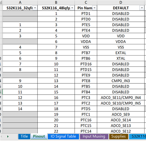
1.Where can I find the pin configuration information related to MSPM0G3507 as shown in the figure.

2.Chips can be downloaded and debugged using SWDIO, SWDCLK,GND and VCC with emulator . In my opinion I think SWD mode is better than BSL mode. Is that so? (BSL does not support debugging)

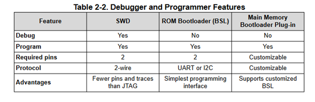
3 If using BSL mode, can only UART0 be used?Can UART1 be used instead?

BR

Haibo

  • Hello Haibo

    The following answers can be for your reference:

    1). You can find the pin configuration information related to MSPM0G3507 in the "Table.6-1 Pin Attributes" of the MSPM03507 Datasheet.

    2). BSL provides a method to program or verify the device memory through a standard UART or I2C serial interface, which makes firmware upgrade not be restricted by debugger. Meanwhile, compared to SWD, BSL is more suitable for firmware upgrade in mass production scenario. In addition, using BSL for update requires a password, which can effectively protect the firmware from malicious damage.

    3). The default ROM BSL program which is burned into the MCU chip by TI is to use UART0 for BSL communication. If you need to use UART1 for communication, you can modify the UART initialization code in the Flash Plug-in program.

    Best Regards,

    Janz Bai