This thread has been locked.

If you have a related question, please click the "Ask a related question" button in the top right corner. The newly created question will be automatically linked to this question.

AM2634: How can I activate other cores in R5FSS0_0?

Part Number: AM2634

To Expert,

I am currently working on activating R5FSS0_1, R5FSS1_0, and R5FSS1_1 in SW where only R5FSS0_0 operates.

Through the SBL example, I understood how to load data from External Flash to RAM and then operate the Core through the SOC_rcmCoreR5FUnhalt function.

Therefore, it is assumed that all necessary data has been loaded into OCRAM.

However, I have a few questions about this:

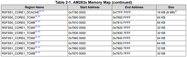
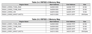
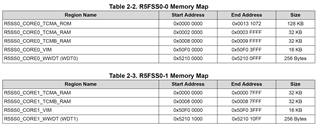
1. I understand initializing TCMA with functions like SOC_rcmStartMemInitTCMA. So how do I write data to TCMA after initialization? I understand that TCMA can only be accessed by each core. Is there another way?

2. Vector seems to be in TCMA, does it act as an EntryPoint? (When you load multi-core imange when debugging SBL, the entry point is set to 0 for the images corresponding to R5FSS0_1, R5FSS1_0, and R5FSS1_1.)

3. Can't I put the Core into a Halt state for testing?

Please reply for a lot of help in development.

Jiung Choi

  • I understand initializing TCMA with functions like SOC_rcmStartMemInitTCMA. So how do I write data to TCMA after initialization? I understand that TCMA can only be accessed by each core. Is there another way?

    The RAM memory can be initialized by using the dedicated auto-initialization hardware. The RAM data memory locations will be initialized to zeros and the corresponding ECC memory is initialized to the correct ECC value for zero. You can write the data directly to the TCMA locations, and no special procedure (for example used for NOR flash) is required. To write data to other core's TCMA, please use the correct memory addresses defined in Memory Map table in TRM. Those memory regions are used by each CPU core to access the TCM memory space of other CPU cores.

    2. Vector seems to be in TCMA, does it act as an EntryPoint? (When you load multi-core imange when debugging SBL, the entry point is set to 0 for the images corresponding to R5FSS0_1, R5FSS1_0, and R5FSS1_1.)

    0x00000000 at TCMA is the reset vector location. The ARM Cortex-R5F processor core starts execution from the reset vector address of 0x00000000 whenever the core gets reset. The EntryPoint is at _c_int00 which may be located in TCMA or OCSRAM. 

    3. Can't I put the Core into a Halt state for testing?

    You can put other cores into halt state (stop fetching instructions).

  • Thank you for your reply.

    I have further inquiries about TCM and boot sequence.

    1. Currently, R5FSS0 operates in Lock-step mode and F5FSS1 operates in Dual-core mode.

    In this case, is it correct that the TCM area allocated to R5FSS0_1 is all used by R5FSS0_0?

    And R5SS0_CORE0_TCMA_ROM overlaps the area. How should I understand it?

    Please explain the TCM area of R5FSS0 in lock-step mode.

    - The area below is Dual-core mode, so it makes sense. (R5FSS1)

    - Please explain how the area below is actually allocated in Lock-step mode and how the overlapping part with R5SS0_CORE0_TCMA_ROM is handled.

    2. In conclusion, can I do the following to activate R5FSS1_0 and R5FSS1_1 in R5FSS0_0?

    - Settings for R5FSS1_0 and R5FSS1_1 (Clock setting, Dual Core mode setting, POR, Memory initialization)

    - Load binaries (Code + Data) to be used in R5FSS1_0 and R5FSS1_1 to L2OCRAM and TCM

    - Unhalt on R5FSS1_0 and R5FSS1_1

    Answers to the above two would be very helpful.

    Thanks

    Jiung Choi

  • 1. Currently, R5FSS0 operates in Lock-step mode and F5FSS1 operates in Dual-core mode.

    In this case, is it correct that the TCM area allocated to R5FSS0_1 is all used by R5FSS0_0?

    And R5SS0_CORE0_TCMA_ROM overlaps the area. How should I understand it?

    Please explain the TCM area of R5FSS0 in lock-step mode

    Yes, you are correct. 

    In Dual Core mode: CORE0 and CORE1 have 64KB of TCM: ( 32KB TCMA  + 32KB TCMB)

    In Lockstep mode: CORE0 has 128KB of TCM. The 64KB TCMA is from 0x00000000 to 0x00100000, or from 0x00020000 to 0x00030000. The 64KB TCMB is from 0x00080000 to 0x00090000. After the boot sequence is complete, both TCMA_ROM and TCMA_RAM are mapped to  a same physical memory (TCMA RAM).

    - Please explain how the area below is actually allocated in Lock-step mode and how the overlapping part with R5SS0_CORE0_TCMA_ROM is handled.

    During boot, the ROM code is copied to TCMA_ROM and executed from TCMA_ROM. 

    After boot sequence is complete, both TCMA_ROM and TCMA_RAM are mapped to  a same physical memory (TCMA RAM). When you write data to 0x00000000, the data is  written to 0x00020000 too.

    2. In conclusion, can I do the following to activate R5FSS1_0 and R5FSS1_1 in R5FSS0_0?

    Yes, you can.

  • QJ Wang,

    thank you for your reply. It helped me a lot.

    Thanks

    Jiung Choi