This thread has been locked.

If you have a related question, please click the "Ask a related question" button in the top right corner. The newly created question will be automatically linked to this question.

MSP432E401Y: SSI used as SPI error when reading data

Part Number: MSP432E401Y

Hello, 

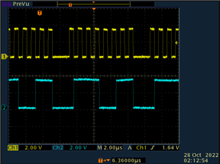
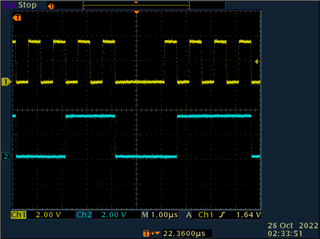
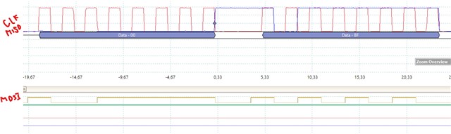
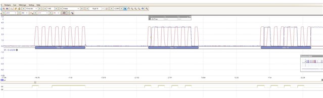
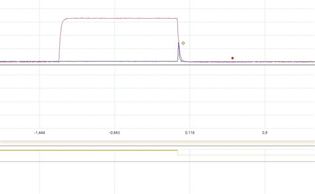
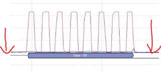
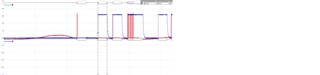
We use SS2 as SPI and try to configure, write and read data from an external flash memory. Everything is working fine but sometimes we read wrong data on MISO from the flash chip. For ex, if we expect 01 02 03 04 05 06 there can be either all data is 00 or some random numbers.

We tried to switch to SS3 but the same problem is still there. We have verified that the clock signal is correct and that the data on MOSI is correct but the flash chip is not responding what we expect occasionally. Can it be that the flash chip is not compatible with this CPU. We use a flash SST26VF064B from another family.

Thank you in advance! 

Regards,

Gergana

  • Hi,

      I'm not familiar with this 3rd party device SST26VF064B. Do you get different results if you lower the SPICLK frequency? Can you repeat the same problem on another board?  Reading the datasheet, the max read frequency is 40Mhz. I'm not sure what SPICLK frequency you have configured for SS2. Please check if you have met all the timing requirements per SST26VF064B like the polarity and phase and baud rate as well as AC characteristics such as data setup and hold times . If you are absolutely sure that the command/data that you send from the master to the slave device is correct and the slave device is not returning the correct data, then please contact SST26VF064B vendor for support. If you believe this is a MCU level issue, please update this thread with additional information. 

  • We used 1 Mb speed and we decreased to 400 000 bps but still the same result. 
    About the polarity and phase, we use mode 0 which is one of the supported by flash. We get erroneous data when we used Mode 3.

    We keep the times for setup, we have delays of 1 ms.

    We have tested on another board with similar results. 

    We connect the flash chip to a launchpad development board and we used osciloscope to measure on the CPU pins for SS2. It was interesting that if we have different capacitance on the CLK pin the data becomes wrong. The probe on the oscilloscope is 10 times and then we have 15 pF and if we change to 1 time the capacitance is 71 pF. In the latter we get wrong data from MISO. It is small values but still influence the communication. 
    Is it something you have noticed? 

  • Hi,

     Can you show the CLK, MOSI and MISO scope captures? is the MISO signal meeting the GPIO Vil and Vih specified in the datasheet and also the SSI Characteristics. 

  • I've used this combination at 60MHz with no surprises. (I used High-Speed Read (0x0B).)

    How are you doing the chip select (Fss)? Using FSSHLDFRM pretty much requires mode=3 (specifically SPH=CPHA=1).

    Also, are you waiting for Tpp (1.5ms) after a write?


  • Hello,

    I am attaching the capture from scope, showing 2 bytes - a CPU command and a byte from flash. This is the same byte of data we are expecting from flash: the byte which the flash chip is sending, once the byte is BF and some time later 00, while the CPU is sending the same data, the command 9F and then a dummy byte AA. 

    The first picture is showing CLK (red), MISO (blue) and MOSI (digital) lines of when data from MISO is correct. The time between a clock cycle is 2.5us and MISO is at around 3V. We have the trigger on the MISO channel at 1V so we can see when the MISO is going up. The pin nCE is already low before the first clock phase, nCE goes low 280us before the clock goes up. 
    On the second picture the communication show wrong data from MISO, we have a clock and the MOSI line seems ok. But we cannot see the MISO line, hence, CPU is reading 00. 

    /Gergana

  • I am using the TI library and configuring the alternate function for Fss pin, with GPIOPinConfigure(GPIO_PD2_SSI2FSS). The pin is set low before data is sent via MOSI. 

    What do you mean by FSSHLDFRM? We tried configuring SSI with mode 3 but we get wrong data. 
    We use the poll the BUSY bit in the status register instead of waiting Tpp. So we continue when the busy is not set.


    It is interesting that we read correct data but sometimes data is wrong, it can be 00, or FF or some random numbers. So something that is sensitive and goes different sometimes. We were thinking if the microprocessor has different behaviour about SSI, but we did not find it in the errata.

    /Gergana

  • Hi Gergana,

      The two screenshots looks the same to me as far as the SPICLK and MOSI are generated. They both show CPU sending 0x9F followed by dummy 0xAA. Reading the SST26VF064B  datasheet, this is a command sequence to read out the JDEC Device ID, correct? The MISO line has proper voltage to meet the Vih and Vil requirements on the MCU side. I don't think the issue is electrical timing related but to be sure you should use a scope rather than a logic analyzer for AC timing analysis.  As you indicated, the second screenshot shows MISO is zero. I don't know what is wrong with the flash device. As far as I can tell, I don't spot anything wrong on the MCU side by looking at the waveforms. Can you repeat the same issue on another board? Are you using the #HOLD? I will suggest you look at the rest of inputs to the flash and make sure there is no noise on them. Please also contact the flash vendor. I hope they can shed some lights too. 

  • Thank you for your reply. We have tested on other boards and we see the same problem. Both on launchpad and our consumer boards.
    This is right, the screenshot is about reading the JEDEC ID. In this case data was 00 but for ex., sometimes it can be 7E 4C 87 instead of BF 26 43. 


    We use the #HOLD and it is set to high every time before we set nCE low and send a command or data to the flash chip. 
    We will contact the flash manufacturer. 

    Another thing we tried was to put the analog scope channels on the MOSI and CLK and change the scope probe for CLK to x1. The the data on MOSI was correct, the capacitance on the probe was not disturbing the data. But if we have the probe on MISO and CLK and we change the probe from 10 times to 1 time (x10 to x1) , meaning we also change the load on the CLK pin, the data the CPU is reading is wrong, or the flash is sending wrong data.

    /Gergana

  • TRM Table 23-2 says that (in Freescale format) Fss is asserted for the duration of a "continuous" transfer. Based on the usage of "continuous" in the rest of the section I concluded that it means "until the FIFO empties". That would mean that, if your software allowed the FIFO to empty in mid-transaction, that transaction would be terminated (Fss deasserted) and the next thing you write would start a new transaction (in the middle).

    I originally used FSSHLDFRM. I later switched to explicit GPIOs, when I added another device to the bus.

  • sometimes it can be 7E 4C 87 instead of BF 26 43. 

    Can you show a scope shot when you are receiving the wrong data instead of all zero's. I can't explain why zero's is received. Perhaps, the 0x9F command wasn't received by the flash device correctly and hence sending back all zeros without a valid command. When you receive 7E 4C 87 instead of BF 26 43, it looks like the master is missing the first bit. This will have something to do with the timing. Show the scope and I hope it will reveal more details. 

  • Hello,

    This is the scope screenshot. 
    Channel A is the MISO, channel B is the clock, D0 is the nCE where it is low before and after we receive data. You are right, data is missing the first byte. Can it be the noise on the CLK pin that is disturbing it, I have the probe with times 1 where the capacitance is 71 pF and it is higher than having the probe times 10. 

  • Here the MOSI line (D3) is added to the picture, sending the command 0x9F and sending dummy bytes. 

    The MISO line is low and I can notice i little upward movement at the end of the last clock cycle of the command but it continues to be low. 

  • I had much higher time resolution on the scope and cpould zoom on the MISO.

    A much closer picture, where MISO is trying to go up at the last clock cycle (after the command 9F is sent by CPU) but goes low again, It goes up to 1.4V.

    And this is where we miss the first bit and we read wrong JEDEC nr. Is it something in the CPU that can cause that, this pin is input for the CPU though. 

  • Hi,

      You are in MODE0, correct? This means the MISO data is sampled on the falling edges of the SSICLK. The max Vil is 0.35*VDD which is equal to 1.15V. If MISO is at 1.4V it may not be sampled as a valid zero by the master. I have gone through the errata document and do not find any relevant errata that can explain this.

      Are you using any other MCU peripherals while you are using SSI? Can you for experiment disable all other peripheral operations except SSI2 to access the flash? I wanted to know if other pins have influence on the MISO pin. 

  • Hello, 

    We are in MODE0. I tried to disable other peripherals, like disabled the communication via I2C and other modules. It did not help. We do not have anything else on the SPI or SSI. 
    Something interesting we noticed is CLK pin from MCU is input when not steered by the clocking cycles, between the bytes the pin is high impedence. We set it as input from the start not to draw current and later configure it as SSI CLK using TI library and it is pin GPIO_PA2_SSI0CLK. Can this be something that destroys the communication? should we have it as output low all other times? 

  • We set it as input from the start not to draw current and later configure it as SSI CLK using TI library and it is pin GPIO_PA2_SSI0CLK. Can this be something that destroys the communication? should we have it as output low all other times? 

    Hi,

      Did you change the driver by any chance? Or you just called the stock APIs GPIOPinConfigure() and GPIOPinTypeSSI()?  GPIOPinTypeSSI()  has the below pin configuration. Can you show your code snippet on how you configure the pins?

    void
    GPIOPinTypeSSI(uint32_t ui32Port, uint8_t ui8Pins)
    {
    //
    // Check the arguments.
    //
    ASSERT(_GPIOBaseValid(ui32Port));

    //
    // Make the pin(s) be peripheral controlled.
    //
    GPIODirModeSet(ui32Port, ui8Pins, GPIO_DIR_MODE_HW);

    //
    // Set the pad(s) for standard push-pull operation.
    //
    GPIOPadConfigSet(ui32Port, ui8Pins, GPIO_STRENGTH_2MA, GPIO_PIN_TYPE_STD);
    }

  • We do not change the stock APIs. We use them as they are.

    We use the defines from Ssi.h, pin_map.h, and other files from the drivers library. We hace frequence for CPU 16 Mhz. And the speed for SPI is 1 Mbps.

    Here is the configuration sequence we use:

    SysCtlPeripheralEnable(SYSCTL_PERIPH_SSI2); 
    SysCtlPeripheralEnable(SYSCTL_PERIPH_GPIOD);

    GPIOPinTypeSSI(GPIO_PORTD_BASE, (GPIO_PIN_0 | GPIO_PIN_1 | GPIO_PIN_3));
    GPIOPinConfigure(GPIO_PD3_SSI2CLK);
    GPIOPinConfigure(GPIO_PD1_SSI2XDAT0); // pin for MOSI
    GPIOPinConfigure(GPIO_PD0_SSI2XDAT1); // pin for MISO

    SSIDisable(SSI2_BASE);
    SSIConfigSetExpClk(SSI2_BASE, _16_MHZ, SSI_FRF_MOTO_MODE_0, SSI_MODE_MASTER, SSI_1_MBPS_SPEED, 8uL);

    SSIAdvModeSet(SSI2_BASE, SSI_ADV_MODE_LEGACY);


  • Hi,

      I don't see anything wrong with your configuration. The problem is more electrical on the MISO pin rather than pin configuration. I'm a bit hesitant to suggest if adding a external pulldown resistor will make a difference on the MISO pin but you can try.  

  • I tried with an internal pulldown from the code and it did not change that we get 00 from MISO instead of data. 

    I wonder if the MCU and SSI can behave differently depending on the batch. 
    We have not seen any problem with a couple boards with same MCU marking that has same flash which has shown error on another MCU. 
    I can read the marking on the two batches MCU chip is different. 

  • I have a question regarding your setup as you said you have the same combination. How do you set the CLK pin, do you have a resistor to GND connected to the pin? 

    We noticed that when the CPU is not clocking bytes the CLK pin is floating, it is high impedence which is strange for a clock pin.

    We configured the CLK pin using the TI driver functions and it is set as clock for SSI2. But when we do not have communication we do not know what the state of the pin is. Even if we set it as output low from the beginning the configuration for SSI is taking over and changing the setting. 

    /Gergana

  • I tried with an internal pulldown from the code and it did not change that we get 00 from MISO instead of data. 

    Hi,

      I was suggesting an external pulldown on MISO not an internal pulldown. 

      Per your waveforms, I don't see the CLK pin floating when it is not clocking in data.

    When you call GPIOPinTypeSSI, the control of the pin (e.g. the direction control) is passed from the GPIO module to the SSI module. 

    void
    GPIOPinTypeSSI(uint32_t ui32Port, uint8_t ui8Pins)
    {
    //
    // Check the arguments.
    //
    ASSERT(_GPIOBaseValid(ui32Port));

    //
    // Make the pin(s) be peripheral controlled.
    //
    GPIODirModeSet(ui32Port, ui8Pins, GPIO_DIR_MODE_HW);

    //
    // Set the pad(s) for standard push-pull operation.
    //
    GPIOPadConfigSet(ui32Port, ui8Pins, GPIO_STRENGTH_2MA, GPIO_PIN_TYPE_STD);

    I wonder if the MCU and SSI can behave differently depending on the batch. 

    That is certainly possible as there could be some variations from chip to chip and wafer to wafer during manufacturing. But I can't explain why this particular chip exhibits this way. I have not seen such a reporting in the past. Since you have several other boards that do not show the issue, I will suggest you do a ABA swap test. This is to make sure the issue is not MCU related. It could be a combination of various things (e.g. soldering, trace capacitance or SST26VF064B or even MCU itself) that caused the issue. 

    The A-B-A Swap Method is a simple cross check test, which can confirm the observed issue is not systemic.

    • A-B-A Swap Method
      (1) Remove the suspected component (A) from the original failing board.
      (2) Replace the suspected component (A) with a known good component (B) and check if the original board now works properly.
      (3) Mount the suspected component (A) to a known good board and see if the same faliure occurs on the good board.

    Step 3 is important because it helps us to exclude any possibility that the issue is caused by a systemic issue or the interaction of multiple slightly bad components on a good board.

  • Hello,

    We tried even with an external pulldown, and there is no effect. 

    We saw the clock line being floating. The red line, Channel B is the CLK.

     .

    Do you know how the SSI modue is setting the CLK pin while there is no data transmission? 

    Thank you for the advice. We will consider it.

    Regards,

    Gergana

  • We saw the clock line being floating. The red line, Channel B is the CLK.

     .

    Hi,

      Can you show the waveform on a good board for the CLK pin. 

    Do you have a chance to perform a ABA swap test?

    Do you know how the SSI modue is setting the CLK pin while there is no data transmission? 

    With SPO=0, the CLK should be low when not transmitting. 

    17.3.7.2 Freescale SPI Frame Format
    The Freescale SPI interface is a four-wire interface where the SSInFss signal behaves as a slave
    select. If operating in Legacy Mode and using the Freescale SPI Frame Format, the inactive state
    and phase of the SSInClk signal are programmable through the SPO and SPH bits in the SSICR0
    control register. If operating in Advanced/Bi-/Quad-SSI mode, the SP0 and SPH bits must be
    programmed to 0.


    SPO Clock Polarity Bit
    When the SPO clock polarity control bit is clear, it produces a steady state Low value on the SSInClk
    pin. If the SPO bit is set, a steady state High value is placed on the SSInClk pin when data is not
    being transferred.


    SPH Phase Control Bit
    The SPH phase control bit selects the clock edge that captures data and allows it to change state.
    The state of this bit has the most impact on the first bit transmitted by either allowing or not allowing
    a clock transition before the first data capture edge. When the SPH phase control bit is clear, data
    is captured on the first clock edge transition. If the SPH bit is set, data is captured on the second
    clock edge transition.

  • Hello, 

    We observe the same on the CLK line. We are not sure if this is potentially leading to undesired behavior. 

    We did a ABA swap test. A flash chip not working on a Launchpad worked on an application board. But we have application boards where we replace the problematic component with a completely new  that had not been used and the same problem appears. 

    Last night we got a wrong data when reading flash even from the board where we had not see this problem before (it has another batch of CPU). 
    This is good at least that we have same behavior. But the problem may appear based on tolerances of the individual board. We continue to try different ways to solve the problem. This issue is new to us as we have not used SSI module before and particularly SSI used as SPI. 

    Changes we made latest:

    we notice that if we have the pins we use for SPI configured in high drive 


    GPIOD->DR8R |= (GPIO_PIN_0 | GPIO_PIN_1|GPIO_PIN_2 | GPIO_PIN_3); 

    We can load more capacitance on CLK pin before the data we read gets wrong. 

    We also have an external resistor of 47 kohm on CLK line and the CLK is more stable.

    Regards,

    Gergana

  • We observe the same on the CLK line. We are not sure if this is potentially leading to undesired behavior. 

    Hi,

      I try to run a simple 1MHz SPI example.  I don't really see the SPICLK fluctuate as in yours especially when it is not transmitting. 

      - Can you check if you have a stable power supply to the MCU and the flash?

      - Is the MCU and the flash on the common ground?

      - Is the trace between the MCU and the flash far?

      - For experiment, can you remove the flash on the board? Will you see SPICLK fluctuate the same as when flash is connected? 

      - Can you repeat the same issue (e.g. reading 0s or reading wrong values) when you use a LaunchPad to read the flash?

    We did a ABA swap test. A flash chip not working on a Launchpad worked on an application board. But we have application boards where we replace the problematic component with a completely new  that had not been used and the same problem appears. 

    I was suggesting a ABA swap test for the MCU. it seems like you swap out the flash rather than the MCU. Is that correct?

    GPIOD->DR8R |= (GPIO_PIN_0 | GPIO_PIN_1|GPIO_PIN_2 | GPIO_PIN_3); 

    I was going to suggest changing the drive strength as well. You could change the drive strength in GPIOPinTypeSSI() API. The default is 2mA. The easiest way is to copy the gpio.c file to your project directory, make the modification to a higher drive strength and rebuild the project. The modified code will take effect over the drivelib library. Or you could change the code and rebuild the driverlib library. 

    void
    GPIOPinTypeSSI(uint32_t ui32Port, uint8_t ui8Pins)
    {
    //
    // Check the arguments.
    //
    ASSERT(_GPIOBaseValid(ui32Port));

    //
    // Make the pin(s) be peripheral controlled.
    //
    GPIODirModeSet(ui32Port, ui8Pins, GPIO_DIR_MODE_HW);

    //
    // Set the pad(s) for standard push-pull operation.
    //
    GPIOPadConfigSet(ui32Port, ui8Pins, GPIO_STRENGTH_2MA, GPIO_PIN_TYPE_STD);

  • - We have stable power to MCU and flash, we checked that. No spike in the power when using SPI. 
    - MCU and flash have the same GND
    - The trace between flash and MCU is very short
    - We have not tried to remove flash and see if the clock line is fluctuating, we can test that. 

    - We have the same issue when reading from the Launchpad. Reading correct data and reading 0s. 

    We have moved a flash from Launchpad and to a board which does not affect the issue any more, it is same behavior. Even when we touch by a finger the MCU pin, the error can appear. 

    Can you try to introduce some extra capacitance on the CLK line by a probe or externally to see if data read from flash is affected? 

    /Gergana

  • Hi Gergana,

      I can try with my LaunchPad next week do some basic SPI operations between a master and a slave. Since I don't have your setup (interfacing to an external flash on a custom board), I doubt I will reproduce the same.

  • Thank you for your inputs. 
    IWe were trying different settings for SPI. If we change the drive strength to 10 mA for the SPI configuration, i.e. in GPIOPinTypeSSI(), we get more stable clock and do not get the error of reading 0s or wrong values of data. Would you recommend that the 10 mA is used for SPI? And can it point to some other issue in electronics as it needs to be so high? 

    In the same function we also change to GPIO_PIN_TYPE_STD_WPD in stead of the standard type. As we understand it, if we have Mode 0, the clock signal is programmed with steady state is low. The clock signal must be programed with a pullup, according to the Note in Tech Ref Manual which refers to steady state high: 


        ''Pullups can be used to avoid unnecessary toggles on the QSSI pins, which can take the
         slave to a wrong state. In addition, if the SSIClk signal is programmed to steady state high
         through the SPO bit in the SSICR0 register, then software must also configure the GPIO port
         pin corresponding to the SSInClk signal as a pullup in the GPIO Pullup Select (GPIOPUR)
         register.'' 

  • We were trying different settings for SPI. If we change the drive strength to 10 mA for the SPI configuration, i.e. in GPIOPinTypeSSI(), we get more stable clock and do not get the error of reading 0s or wrong values of data. Would you recommend that the 10 mA is used for SPI? And can it point to some other issue in electronics as it needs to be so high? 

    Hi Gergana,

    While I'm glad to see a higher drive strength somehow resolves your issue, I don't understand why as high as 10mA is needed  if the capacitive load is not huge. Earlier, you said you have a minimum distance between the MCU and the flash.  As far as I know, 2mA buffer strength which is being used by default in the GPIOPinTypeSSI is good for majority of customers. You are the first customer to require a 10mA for what I can remember. I don't really see an issue to change to 10mA but it will increase your current draw. 

     I will suggest you use 10x on your probe to reduce the overall capacitive load when probing the signal on the scope. Earlier you said you measured 15pF which is within the reach of 2mA buffer at a slower rise/fall time. Using 10mA to drive a 15pF load will create a much sharper edge on rise/fall. 

    In the same function we also change to GPIO_PIN_TYPE_STD_WPD in stead of the standard type. As we understand it, if we have Mode 0, the clock signal is programmed with steady state is low. The clock signal must be programed with a pullup, according to the Note in Tech Ref Manual which refers to steady state high: 


        ''Pullups can be used to avoid unnecessary toggles on the QSSI pins, which can take the
         slave to a wrong state. In addition, if the SSIClk signal is programmed to steady state high
         through the SPO bit in the SSICR0 register, then software must also configure the GPIO port
         pin corresponding to the SSInClk signal as a pullup in the GPIO Pullup Select (GPIOPUR)
         register.'' 

    You are correct that GPIO_PIN_TYPE_STD_WPD is recommended if the SPO in the SSICR0 register is set to high. However, you are operating in Mode 0 which doesn't really require GPIO_PIN_TYPE_STD_WPD. 

  • Thank you. We checked an example code here:

    https://dev.ti.com/tirex/explore/node?node=A__AK4Mx17LHgMZFoRl0XdckQ__com.ti.SIMPLELINK_MSP432E4_SDK__J4.hfJy__LATEST

    where the drive strength is also higher than the default of 2 mA, GPIOB->DR8R |= (GPIO_PIN_5 | GPIO_PIN_4); 

  • Hi Gergana,

      Thank you for crossing checking the drive strength on the MSP432E device for serial flash operation.  I suppose during serial flash example development, they must have noticed the effect of the default drive strength and manually changed to up the strength to solve perhaps a similar problem that you were facing. This is new to me. I will bookmark this post for future reference. Thanks again. 

    /* No driverlib API to only set the GPIO high drive setting, so we use
    * bare metal */
    GPIOB->DR8R |= (GPIO_PIN_5 | GPIO_PIN_4);
    GPIOD->DR8R |= (GPIO_PIN_5 | GPIO_PIN_4);
    GPIOE->DR8R |= (GPIO_PIN_5 | GPIO_PIN_4);

  • Thank you for your support on our case. 

    Regards,

    Gergana