This thread has been locked.

If you have a related question, please click the "Ask a related question" button in the top right corner. The newly created question will be automatically linked to this question.

AM2634: Power net decoupling recommendation discrepancy between HW Design Guide and LP-AM263

Part Number: AM2634
Other Parts Discussed in Thread: LP-AM263

Hey Sitara MCU team,

I have a customer working on their HW implementation for a new design based on the AM2634 and they noticed a discrepancy between the recommended decoupling circuitry in the HW Design Guide (SPRABJ8A) versus the actual Launchpad design (LP-AM263).

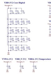
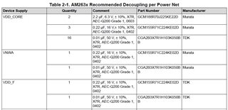
One specific discrepancy that I can point out is the guidance provided for handling VDD_CORE. In Table 2-1 of the design guide it recommends 16x 0.01uF, 3x 0.22uF, and 2x 2.2uF capacitors for VDD_CORE but if you look at the same document in Figure 2-5 along with the actual LP-AM263 PROC111E2 schematic you'll see that the actual decoupling capacitors used on this node (VDD_AM263_1V2) are different. Similar discrepancies can also be seen for other rails like VNWA and VDD_F. See below for reference!

Our question is...which design guidance is correct and should be followed? 

1.2V Decoupling Circuitry on LP-AM263:

1.2V Decoupling Recommendation from HW Design Guide:

Thanks for your help with clearing this up!

Best regards,

Matt Calvo

  • Hi Matt, 

    All of these are valid capacitor recommendations and you will likely not see an issue using any of them. Background: 

    In both the controlCard EVM design and LaunchPad EVM design I started with design with the number and value of capacitors as seen in the referenced Table 2-1. Once I had a fully routed power distribution network (PDN) I did additional 3D simulations to extract the Z11 (package looking into PCB) for the resulting PCB + decoupling network. I ran with different decoupling values to see which set of values gave me the best PDN performance (lower impedance over widest frequency range, minimized plane resonances). 

    If PDN simulation is possible, I would recommend starting with these table values and then adjusting as necessary to get best performance on your specific PCB stack/layout. But if no simulation of your specific PCB is possible, I would try to replicate either the controlCard or LaunchPad layout and the specific capacitor set used. The LaunchPad is a 6-layer design, while the controlCard is a 10 layer design. I saw different PCB plane and package resonance simulation results between the two designs. 

    In any case: after the hardware is available, I would then follow-up by putting an oscilloscope (at least 500 MHz BW, ideally a differential probe) on the 1.2V core and 3.3V planes near the BGA to verify the transient performance of the system with specific software loading you are running. Best probing can be done by depopulating one of the decoupling capacitor under the center of the BGA and measuring across the pads. Final capacitor values can then be experimentally chosen based on actual performance of the system. 

    Let me know if that helps. 

    Thank you,

    -Randy