Hi team,
My customer is considering TM4C1299NCZAD with our new design board.
They are considering TM4C1299NCZAD for their new design board.
They are studying whether it is possible to use EPI or Quad-SSI for communication interface between TI microcontroller and FPGA to control memory mapped,
■ Questions
1) Is memory mapped control possible with Quad-SSI?
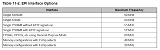
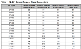
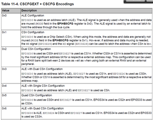
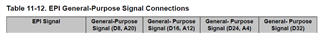
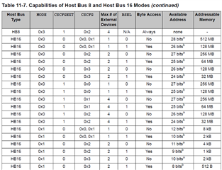
2) According to the data sheet, it seems that EPI can set 8/16/32-bit parallel bus.
What is the number of IO used for EPI 8-bit, 16-bit, and 32-bit? (Sorry, I checked the datasheet, but I didn't really understand how to read it.)
The communication format and the number of IO will change depending on the option settings such as SDRAM and SRAM,
but they are considering EPI 8bit to reduce the number of IO while providing high-speed access.