This thread has been locked.

If you have a related question, please click the "Ask a related question" button in the top right corner. The newly created question will be automatically linked to this question.

TMS570LC4357: Safe-TI demo application is mssing hardware register definitions

Part Number: TMS570LC4357
Other Parts Discussed in Thread: HALCOGEN

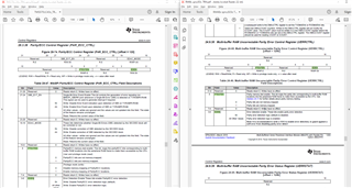
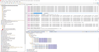
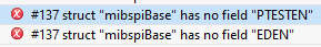
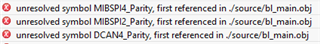
When I compile the demo for this processor, there are references in parity_functions.c to undefined test registers canREG1->TEST, mibspi1->PTESTEN, mibspi3->EDEN.  These are defined in the demos for other TMS570 processors and for RM42x,RM46x, RM48x. Do these registers exist in TMS570LC4357 or should these tests be excluded?

  • Hi Darryl,

    Do these registers exist in TMS570LC4357 or should these tests be excluded?

    They were included in TMS570LC4357 as well:

    --

    Thanks & regards,
    Jagadish.

  • Jagadish,

      Thank you for the quick response.  Your attached illustrations are a tiny graphic that is not readable.  Can you tell me the specific pages/sections  of the TRM or data sheet and the version number of your document?  Is there an update to the SAFE-TI zip file for TMS570LC4357  that provides the missing definitions?

    Darryl

  • Jagadish,

        Also missing, a whole set of definitions in HL_mibspi.h for MIBSPI1, that are defined for MIBSPI2,3,4,5, for example MIBSPI2_PAR_ECC_CTRL_CONFIGVALUE.  And in parity_functions.c there is no code for DCAN4_Parity, although there is for DCAN1,2,3. Thirdly, There is code for MIBSPI1_Parity and MINSPI3_Parity and MIBSPI5_Parity but not for MIBSPI2 and MIBSPI4.  If I have to modify the SafeTI code, that seems to defeat  the purpose of using a pre-defined Safe-TI library.

  • Hi Darryl,

    Also missing, a whole set of definitions in HL_mibspi.h for MIBSPI1, that are defined for MIBSPI2,3,4,5, for example MIBSPI2_PAR_ECC_CTRL_CONFIGVALUE.

    It is there, right? Look at below pic:

    And in parity_functions.c there is no code for DCAN4_Parity, although there is for DCAN1,2,3. Thirdly, There is code for MIBSPI1_Parity and MINSPI3_Parity and MIBSPI5_Parity but not for MIBSPI2 and MIBSPI4.  If I have to modify the SafeTI code, that seems to defeat  the purpose of using a pre-defined Safe-TI library.

    I am unable to find them, can you please provide screenshots for better understanding.

    --
    Thanks & regards,
    Jagdish.

  • Jagadish,

    There are 3 issues, Two may be HALCoGen failure. I am using HALCoGen 4.07.01.  Missing register definitions in a structure, missing code in parity_functions.c, and missing assembly language code in HL_sys_core.asm

    #1. Missing register definitions

        It is difficult to provide screen shots of things that are missing.  Here are the errors

    Here is the definition from HALCoGen/TMS570LC43x/include/HL_reg_mibspi.h

    /** @typedef mibspiBASE_t
    * @brief MIBSPI Register Frame Type Definition
    *
    * This type is used to access the MIBSPI Registers.
    */
    typedef volatile struct mibspiBase
    {
    uint32 GCR0; /**< 0x0000: Global Control 0 */
    uint32 GCR1; /**< 0x0004: Global Control 1 */
    uint32 INT0; /**< 0x0008: Interrupt Register */
    uint32 LVL; /**< 0x000C: Interrupt Level */
    uint32 FLG; /**< 0x0010: Interrupt flags */
    uint32 PC0; /**< 0x0014: Function Pin Enable */
    uint32 PC1; /**< 0x0018: Pin Direction */
    uint32 PC2; /**< 0x001C: Pin Input Latch */
    uint32 PC3; /**< 0x0020: Pin Output Latch */
    uint32 PC4; /**< 0x0024: Output Pin Set */
    uint32 PC5; /**< 0x0028: Output Pin Clr */
    uint32 PC6; /**< 0x002C: Open Drain Output Enable */
    uint32 PC7; /**< 0x0030: Pullup/Pulldown Disable */
    uint32 PC8; /**< 0x0034: Pullup/Pulldown Selection */
    uint32 DAT0; /**< 0x0038: Transmit Data */
    uint32 DAT1; /**< 0x003C: Transmit Data with Format and Chip Select */
    uint32 BUF; /**< 0x0040: Receive Buffer */
    uint32 EMU; /**< 0x0044: Emulation Receive Buffer */
    uint32 DELAY; /**< 0x0048: Delays */
    uint32 DEF; /**< 0x004C: Default Chip Select */
    uint32 FMT0; /**< 0x0050: Data Format 0 */
    uint32 FMT1; /**< 0x0054: Data Format 1 */
    uint32 FMT2; /**< 0x0058: Data Format 2 */
    uint32 FMT3; /**< 0x005C: Data Format 3 */
    uint32 INTVECT0; /**< 0x0060: Interrupt Vector 0 */
    uint32 INTVECT1; /**< 0x0064: Interrupt Vector 1 */
    uint32 rsvd3; /**< 0x0068: Slew Rate Select */
    uint32 PMCTRL; /**< 0x006C: Parallel Mode Control */
    uint32 MIBSPIE; /**< 0x0070: Multi-buffer Mode Enable */
    uint32 TGITENST; /**< 0x0074: TG Interrupt Enable Set */
    uint32 TGITENCR; /**< 0x0078: TG Interrupt Enable Clear */
    uint32 TGITLVST; /**< 0x007C: Transfer Group Interrupt Level Set */
    uint32 TGITLVCR; /**< 0x0080: Transfer Group Interrupt Level Clear */
    uint32 TGINTFLG; /**< 0x0084: Transfer Group Interrupt Flag */
    uint32 rsvd1[2U]; /**< 0x0088: Reserved */
    uint32 TICKCNT; /**< 0x0090: Tick Counter */
    uint32 LTGPEND; /**< 0x0090: Last TG End Pointer */
    uint32 TGCTRL[16U]; /**< 0x0098 - 0x00D4: Transfer Group Control */
    uint32 DMACTRL[8U]; /**< 0x00D8 - 0x00F4: DMA Control */
    uint32 DMACOUNT[8U]; /**< 0x00F8 - 0x0114: DMA Count */
    uint32 DMACNTLEN; /**< 0x0118 - 0x0114: DMA Control length */
    uint32 rsvd2; /**< 0x011C: Reserved */
    uint32 PAR_ECC_CTRL; /**< 0x0120: Multi-buffer RAM Uncorrectable Parity Error Control */
    uint32 UERRSTAT; /**< 0x0124: Multi-buffer RAM Uncorrectable Parity Error Status */
    uint32 UERRADDRRX; /**< 0x0128: RXRAM Uncorrectable Parity Error Address */
    uint32 UERRADDRTX; /**< 0x012C: TXRAM Uncorrectable Parity Error Address */
    uint32 RXOVRN_BUF_ADDR; /**< 0x0130: RXRAM Overrun Buffer Address */
    uint32 IOLPKTSTCR; /**< 0x0134: IO loopback */
    uint32 EXT_PRESCALE1; /**< 0x0138: SPI Extended Prescale Register 1*/
    uint32 EXT_PRESCALE2; /**< 0x013C: SPI Extended Prescale Register 2*/
    uint32 ECCDIAG_CTRL; /**< 0x0140: ECC Diagnostic Control register*/
    uint32 ECCDIAG_STAT; /**< 0x0144: ECC Diagnostic Status register*/
    uint32 SBERRADDR1; /**< 0x0148: */
    uint8 rsvd4[6]; /**< 0x014C-0x152: Single Bit Error Address Register - RXRAM*/
    uint32 SBERRADDR0; /**< 0x0152: Single Bit Error Address Register - TXRAM*/

    } mibspiBASE_t;

    #2 Missing MibSPI and DCAN4 functions--------------------

    In the TMS570LC43x path: C:\ti\Hercules\Hercules Safety MCU Demos\4.0.0\TMS570LC43x_target_sources\

    These three are present: MIBSPI1_Parity(), MIBSPI3_Parity(), MIBSPI5_Parity().
    parity_functions.c does not contain MIBSPI2_Parity(), MIBSPI4_Parity().

    These three are present: DCAN1_Parity(), DCAN2_Parity(), DCAN3_Parity().
    parity_functions.c does not contain DCAN4_Parity()

    void DCAN1_Parity(void)
    {
    unsigned int *mailbox;

    /** - Fill MailBox data with 0 */
    canREG1->IF1DATx[0] = 0;
    canREG1->IF1DATx[1] = 0;
    canREG1->IF1DATx[2] = 0;
    canREG1->IF1DATx[3] = 0;
    canREG1->IF1DATx[4] = 0;
    canREG1->IF1DATx[5] = 0;
    canREG1->IF1DATx[6] = 0;
    canREG1->IF1DATx[7] = 0;

    /** - Initialize Command Registers and select Message Number 1 */
    canREG1->IF1CMD = 0xFF;
    canREG1->IF1NO = 1;

    /** - wait for Busy Flag to set, IF[1] contents will be moved to Mailbox 1 */
    while((canREG1->IF1STAT & 0x80) == 0x80);

    /** - Disable Parity PMD = 0x5 */
    canREG1->CTL |= 0x00001400;

    /** - Enable Test Mode */
    canREG1->CTL |= 0x80;

    /** - Enable Direct Access to DCAN RAM */
    canREG1->TEST |= 0x200;

    /** - Corrupt Mail Box1 data locations to generate Parity Error */
    mailbox = (unsigned int*)(canMEM1+ 0x20);
    *mailbox = *mailbox | 1;

    /** - Disable Direct access to DCAN RAM */
    canREG1->TEST &= 0xFFFFFDFF;

    /** - Enter Init Mode and Disable Test Mode and Enable Parity*/
    canREG1->CTL &= 0xFFFFEB7E;

    /** - Configure the Transfer direction to be from the
    * message object 1 to the IF1 Register and start the read */
    canREG1->IF1CMD = 0x7F;
    canREG1->IF1NO = 1;

    /** - wait for Busy Flag to set, Mailbox[1] contents will be moved to IF[1] */
    while((canREG1->IF1STAT & 0x80) == 0x80);

    /* Wait for the DCAN Parity Error Bit to get set */
    while((canREG1->ES & 0x100) != 0x100);

    }

    /** @fn void DCAN2_Parity(void)
    * @brief DCAN 2 Parity Error creation and check routines.
    */

    void DCAN2_Parity(void)
    {
    unsigned int *mailbox;

    /** - Fill MailBox data with 0 */
    canREG2->IF1DATx[0] = 0;
    canREG2->IF1DATx[1] = 0;
    canREG2->IF1DATx[2] = 0;
    canREG2->IF1DATx[3] = 0;
    canREG2->IF1DATx[4] = 0;
    canREG2->IF1DATx[5] = 0;
    canREG2->IF1DATx[6] = 0;
    canREG2->IF1DATx[7] = 0;

    /** - Initialize Command Registers and select Message Number 1 */
    canREG2->IF1CMD = 0xFF;
    canREG2->IF1NO = 1;

    /** - wait for Busy Flag to set, IF[1] contents will be moved to Mailbox 1 */
    while((canREG2->IF1STAT & 0x80) == 0x80);

    /** - Disable Parity PMD = 0x5 */
    canREG2->CTL |= 0x00001400;

    /** - Enable Test Mode */
    canREG2->CTL |= 0x80;

    /** - Enable Direct Access to DCAN RAM */
    canREG2->TEST |= 0x200;

    /** - Corrupt Mail Box1 data locations to generate Parity Error */
    mailbox = (unsigned int*)(canMEM2+ 0x20);
    *mailbox = *mailbox | 1;

    /** - Disable Direct access to DCAN RAM */
    canREG2->TEST &= 0xFFFFFDFF;

    /** - Enter Init Mode and Disable Test Mode and Enable Parity*/
    canREG2->CTL &= 0xFFFFEB7E;

    /** - Configure the Transfer direction to be from the
    * message object 1 to the IF1 Register and start the read */
    canREG2->IF1CMD = 0x7F;
    canREG2->IF1NO = 1;

    /** - wait for Busy Flag to set, Mailbox[1] contents will be moved to IF[1] */
    while((canREG2->IF1STAT & 0x80) == 0x80);

    /* Wait for the DCAN Parity Error Bit to get set */
    while((canREG2->ES & 0x100) != 0x100);

    }

    /** @fn void DCAN3_Parity(void)
    * @brief DCAN 3 Parity Error creation and check routines.
    */
    void DCAN3_Parity(void)
    {
    unsigned int *mailbox;

    /** - Fill MailBox data with 0 */
    canREG3->IF1DATx[0] = 0;
    canREG3->IF1DATx[1] = 0;
    canREG3->IF1DATx[2] = 0;
    canREG3->IF1DATx[3] = 0;
    canREG3->IF1DATx[4] = 0;
    canREG3->IF1DATx[5] = 0;
    canREG3->IF1DATx[6] = 0;
    canREG3->IF1DATx[7] = 0;

    /** - Initialize Command Registers and select Message Number 1 */
    canREG3->IF1CMD = 0xFF;
    canREG3->IF1NO = 1;

    /** - wait for Busy Flag to set, IF[1] contents will be moved to Mailbox 1 */
    while((canREG3->IF1STAT & 0x80) == 0x80);

    /** - Disable Parity PMD = 0x5 */
    canREG3->CTL |= 0x00001400;

    /** - Enable Test Mode */
    canREG3->CTL |= 0x80;

    /** - Enable Direct Access to DCAN RAM */
    canREG3->TEST |= 0x200;

    /** - Corrupt Mail Box1 data locations to generate Parity Error */
    mailbox = (unsigned int*)(canMEM3+ 0x20);
    *mailbox = *mailbox | 1;

    /** - Disable Direct access to DCAN RAM */
    canREG3->TEST &= 0xFFFFFDFF;

    /** - Enter Init Mode and Disable Test Mode and Enable Parity*/
    canREG3->CTL &= 0xFFFFEB7E;

    /** - Configure the Transfer direction to be from the
    * message object 1 to the IF1 Register and start the read */
    canREG3->IF1CMD = 0x7F;
    canREG3->IF1NO = 1;

    /** - wait for Busy Flag to set, Mailbox[1] contents will be moved to IF[1] */
    while((canREG3->IF1STAT & 0x80) == 0x80);

    /* Wait for the DCAN Parity Error Bit to get set */
    while((canREG3->ES & 0x100) != 0x100);

    }

    /** @fn void MIBSPI1_Parity(void)
    * @brief MIBSPI 1 RAM Parity Error creation and check routines.
    */
    void MIBSPI1_Parity(void)
    {
    unsigned short data[8]= {0x1234,0x2345,0x3456,0x4567,0x5678,0x6789,0x789A,0x89AB};
    unsigned char *TXRamParity = (unsigned char *)(mibspiRAM1) + 0x400;

    /** - Initialize MIBSPI Module */
    mibspiInit();

    /** - Initialize Data Buffer */
    mibspiSetData(mibspiREG1, 0, data);

    /** - Memory Map parity bits */
    //mibspiREG1->PTESTEN = 1;
    ((mibspi_par_ecc_reg_t*)&mibspiREG1->PAR_ECC_CTRL)->PTESTEN = 1;

    /** - Disable paritt error detection logic */
    //mibspiREG1->EDEN = 0x5;
    ((mibspi_par_ecc_reg_t*)&mibspiREG3->PAR_ECC_CTRL)->EDEN = 5;

    /** - Introduce Parity Error by flipping one bit in TXRAM parity */
    TXRamParity++;
    TXRamParity++;
    *TXRamParity = ~(*TXRamParity);

    /** - Enable paritt error detection logic */
    //mibspiREG1->EDEN = 0xA;
    ((mibspi_par_ecc_reg_t*)&mibspiREG1->PAR_ECC_CTRL)->EDEN = 0x0A;

    /** - Remove Memory Map of parity bits */
    //mibspiREG1->PTESTEN = 0;
    ((mibspi_par_ecc_reg_t*)&mibspiREG1->PAR_ECC_CTRL)->PTESTEN = 0;

    /** - Trigger the transfer group0, since Parity is corrupted Parity
    * error will be triggered */
    mibspiTransfer(mibspiREG1, 0);

    asm(" nop");
    asm(" nop");
    asm(" nop");

    /** Reset SPI once Test is complete */
    mibspiREG1->GCR0 = 0U;


    }

    /** @fn void MIBSPI3_Parity(void)
    * @brief MIBSPI 3 RAM Parity Error creation and check routines.
    */
    void MIBSPI3_Parity(void)
    {
    unsigned short data[8]= {0x1234,0x2345,0x3456,0x4567,0x5678,0x6789,0x789A,0x89AB};
    unsigned char *TXRamParity = (unsigned char *)(mibspiRAM3) + 0x400;

    /** - Initialize MIBSPI Module */
    mibspiInit();

    /** - Initialize Data Buffer */
    mibspiSetData(mibspiREG3, 0, data);

    /** - Memory Map parity bits */
    //mibspiREG3->PTESTEN = 1;
    ((mibspi_par_ecc_reg_t*)&mibspiREG3->PAR_ECC_CTRL)->PTESTEN = 1;

    /** - Disable paritt error detection logic */
    //mibspiREG3->EDEN = 0x5;
    ((mibspi_par_ecc_reg_t*)&mibspiREG3->PAR_ECC_CTRL)->EDEN = 5;

    /** - Introduce Parity Error by flipping one bit in TXRAM parity */
    TXRamParity++;
    TXRamParity++;
    *TXRamParity = ~(*TXRamParity);

    /** - Enable paritt error detection logic */
    //mibspiREG3->EDEN = 0xA;
    ((mibspi_par_ecc_reg_t*)&mibspiREG3->PAR_ECC_CTRL)->EDEN = 0x0A;

    /** - Remove Memory Map of parity bits */
    //mibspiREG3->PTESTEN = 0;
    ((mibspi_par_ecc_reg_t*)&mibspiREG3->PAR_ECC_CTRL)->PTESTEN = 0;

    /** - Trigger the transfer group0, since Parity is corrupted Parity
    * error will be triggered */
    mibspiTransfer(mibspiREG3, 0);

    asm(" nop");
    asm(" nop");
    asm(" nop");

    /** Reset SPI once Test is complete */
    mibspiREG3->GCR0 = 0U;

    }

    /** @fn void MIBSPIP5_Parity(void)
    * @brief MIBSPI 5 RAM Parity Error creation and check routines.
    */
    void MIBSPI5_Parity(void)
    {
    unsigned short data[8]= {0x1234,0x2345,0x3456,0x4567,0x5678,0x6789,0x789A,0x89AB};
    unsigned char *TXRamParity = (unsigned char *)(mibspiRAM5) + 0x400;

    /** - Initialize MIBSPI Module */
    mibspiInit();

    /** - Initialize Data Buffer */
    mibspiSetData(mibspiREG5, 0, data);

    /** - Memory Map parity bits */
    //mibspiREG5->PTESTEN = 1;
    ((mibspi_par_ecc_reg_t*)&mibspiREG5->PAR_ECC_CTRL)->PTESTEN = 1;
    /** - Disable paritt error detection logic */
    //mibspiREG5->EDEN = 0x5;
    ((mibspi_par_ecc_reg_t*)&mibspiREG5->PAR_ECC_CTRL)->EDEN = 5;

    /** - Introduce Parity Error by flipping one bit in TXRAM parity */
    TXRamParity++;
    TXRamParity++;
    *TXRamParity = ~(*TXRamParity);

    /** - Enable paritt error detection logic */
    //mibspiREG5->EDEN = 0xA;
    ((mibspi_par_ecc_reg_t*)&mibspiREG5->PAR_ECC_CTRL)->EDEN = 0x0A;

    /** - Remove Memory Map of parity bits */
    //mibspiREG5->PTESTEN = 0;
    ((mibspi_par_ecc_reg_t*)&mibspiREG5->PAR_ECC_CTRL)->PTESTEN = 0;

    /** - Trigger the transfer group0, since Parity is corrupted Parity
    * error will be triggered */
    mibspiTransfer(mibspiREG5, 0);

    asm(" nop");
    asm(" nop");
    asm(" nop");

    /** Reset SPI once Test is complete */
    mibspiREG5->GCR0 = 0U;

    }

    /** @fn void MIBADC2_Parity(void)
    * @brief MIBADC 2 Parity Error creation and check routines.
    */
    void MIBADC2_Parity(void)

    #3 Missing ASM functions -----------------------------

    The coreEnableFlashEcc() and coreDisableFlashEcc() are present in the HL_sys_core.asm for other processors but not present in the TMS570LC43x branch.  I have not found a HALCoGen setting that causes them to be generated.

  • Hi Darryl,

    When i build Safe-TI demo for TMS570LC4357 on my PC, i didn't see any of the errors you are talking about.

    You can see my build result. So, i don't understand why you are getting all those errors. Which version of safe-TI demo you are compiling? and did you made any changes to it?

    --
    Thanks & regards,
    Jagadish.

  • Jagadish,

        I am using version 2.4.0.  I Did make one major change.  IN THE DISTRIBUTION, ALL OF THE CODE (100%) IN PARITY_FUNCTION.C IS IF(0) REMOVED.  I re-enabled it.  This is why I asked earlier, if the hardware supported these functions. Change the if(0) to if(1) to see the errors.

  • The coreEnableFlashEcc() and coreDisableFlashEcc() are present in the HL_sys_core.asm for other processors but not present in the TMS570LC43x branch.  I have not found a HALCoGen setting that causes them to be generated.

    The ECC logic for the program flash is enabled at reset, and cannot be disabled.

  •     It is difficult to provide screen shots of things that are missing.  Here are the errors

    Here is the definition from HALCoGen/TMS570LC43x/include/HL_reg_mibspi.h

    The PTESTEN and EDEN are two bit-fields of PAR_ECC_CTRL register. In HalCoGen code and SDL APIs, we define the register as a 32-bit register, and don't break it down to bit fields structure. 

  • And in parity_functions.c there is no code for DCAN4_Parity, although there is for DCAN1,2,3. Thirdly, There is code for MIBSPI1_Parity and MINSPI3_Parity and MIBSPI5_Parity but not for MIBSPI2 and MIBSPI4.  If I have to modify the SafeTI code, that seems to defeat  the purpose of using a pre-defined Safe-TI library.

    HalCoGen doesn't generate those files for TMS570LC43x device. You can use SDL for performing MibSPI and DCAN RAM ECC selftest test.

    For example:

    SL_SelfTest_MibSPI(MIBSPI_ECC_TEST_MODE_1BIT, SL_MIBSPI4);

    SL_SelfTest_CAN(CAN_ECC_TEST_MODE_1BIT_FAULT_INJECT, SL_DCAN4);

  • In the demo code for TMS570LC43x, in flash.c the ATCM_Correctable_Error() function references coreDisableFlashECC() and coreEnableFlashECC();.

    C:\ti\Hercules\Hercules Safety MCU Demos\4.0.0\TMS570LC43x_target_sources\demo-app\source\flash.c 

    Is this not the correct demo code for my TMS570LC4357?

  • Thank you for pointing this out.

    ATCM_Correctable_Error(void) should not be used for TMS570LC43x and RM57Lx. Those two devices are Cortex-R5F based ARM MCU, and all other devices are Cortex-R4F based devices. The ECC logic for flash on Cortex-R4F devices can be enabled/disabled, and ECC space can be written manually (for error injection). But for Cortex-R5F, we use different ways to inject ECC error.

    Please use the Safety Diagnostic Lib instead of the dmeo examples.

  • I see that example_SafetyLib.c has a more complete list of self tests.  This is what I was looking for.

  • Do you know where I can find definitions for RAMTYPE_NHET2 | RAMTYPE_HET_TU2 | RAMTYPE_MIBADC1_RAM |
    RAMTYPE_MIBADC2_RAM  ?  These are specific to TMS570LC43x but not defined.

  • They are defined in sl_types.h

    The memory group numbers are defined in datasheet: Table 6-34. Memory Initialization

  • Sorry, I was using the wrong sl_types.h file from a different processor. Resolved now.