This thread has been locked.

If you have a related question, please click the "Ask a related question" button in the top right corner. The newly created question will be automatically linked to this question.

AM2634-Q1: Baud rate clock not correct in dual LIN bus transmission

Part Number: AM2634-Q1
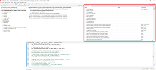
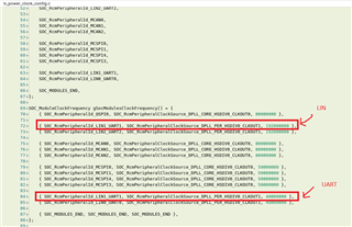
Other Parts Discussed in Thread: SYSCONFIG

Dear Expert.

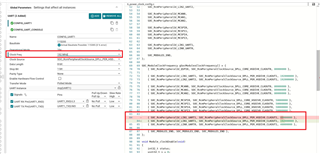
Customer try to write a program for dual LIN TX.

LIN1(B9/A9) & LIN2 (A8/B8) use same baud rate (19200) to shoot same 6 bytes data. Even we declare same baud rate parameter in code, but we found LIN1 & LIN2 is still base on different baud rate (clock) for data transmission. We not sure what's something wrong.

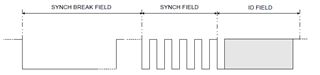
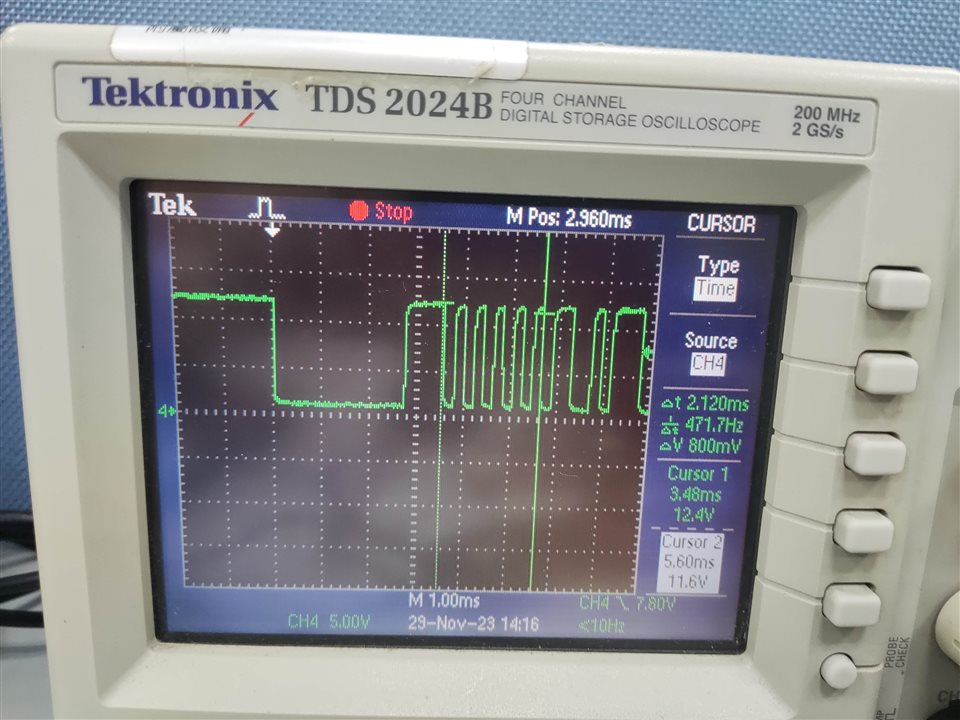
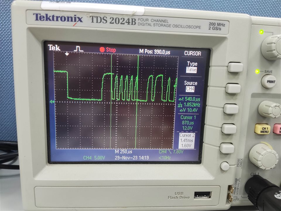
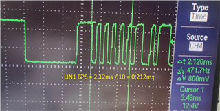
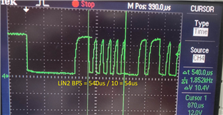
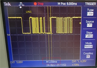
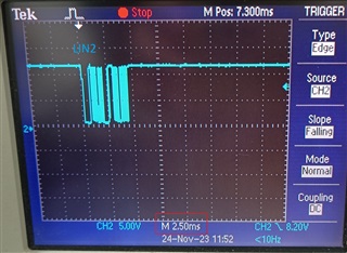
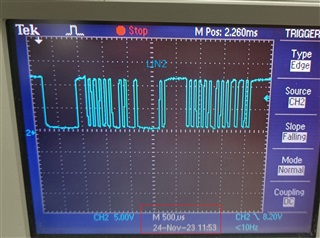
Capture graph as below, 

The clock is not the same obviously!

(1) LIN 1, 19200, 2.5ms/DIV

(2) LIN2, 19200 ?!, 2.5ms/DIV

(2) LIN2, 19200 ?!, 500us/DIV
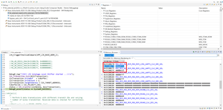
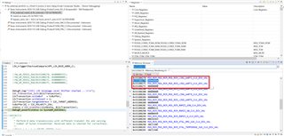
Code as below.

LIN1:

#define FRAME_LENGTH        (0x8)
#define LIN_ID              (0x10)

#define LIN_PASS            (0xABCD)
#define LIN_FAIL            (0xFFFF)

#define APP_LIN1_BASE_ADDR   (CONFIG_LIN1_BASE_ADDR)
#define APP_LIN2_BASE_ADDR   (CONFIG_LIN2_BASE_ADDR)

/* Globals */
uint16_t result;
uint16_t txData[8] = {0x12, 0x34, 0x56, 0x78, 0x9A, 0xAB, 0xCD, 0xEF};
uint16_t txxData[8] = {0x00, 0xFF, 0x55, 0xAA, 0xFF, 0x00, 0xAA, 0x55};
uint16_t rxData[8] = {0x00};

/* lin_external_main */
void lin1_tx_test(void)
{
    uint32_t                i;
    uint16_t                txID, error = 0;
    int32_t                 status;
    uint8_t                 txBuffer[1];

    /* Open drivers to open the UART driver for console */

    ti_Console_print("[LIN1] LIN mode external, application started ...\r\n");

    /* Enable parity check */
    LIN_enableParity(APP_LIN1_BASE_ADDR);

    /* Enable multi-buffer mode */
    LIN_enableMultibufferMode(APP_LIN1_BASE_ADDR);

    /* Enable Fixed baud rate mode */
    LIN_disableAutomaticBaudrate(APP_LIN1_BASE_ADDR);

    /* Reaching the Baud of 19200 */
    LIN_setBaudRatePrescaler(APP_LIN1_BASE_ADDR, 624U, 0U);

    /* Enable transfer of data to the shift registers  */
    LIN_enableDataTransmitter(APP_LIN1_BASE_ADDR);

    /* Enable the triggering of checksum compare on extended frames */
    LIN_triggerChecksumCompare(APP_LIN1_BASE_ADDR);

    ti_Console_print("LIN1 Volatage Level Shifter started ...\r\n");

    /*
     * Perform 8 data transmissions with different transmit IDs and varying
     * number of bytes transmitted. Received data is checked for correctness.
     */
//    for(i = 1 ; i <= FRAME_LENGTH; i++)
//    {
    i = 6;
        /* Create a new transmit ID and update with parity bits */
        txID = (LIN_ID + i);
        txID = LIN_generateParityID(txID);

        /*
         * Set the frame length (number of bytes to be transmitted)
         */
        LIN_setFrameLength(APP_LIN1_BASE_ADDR, i);

        /*
         * This places data into the transmit buffer.
         * No ID or data is placed on the bus and transmitted yet.
         */
        LIN_sendData(APP_LIN1_BASE_ADDR, txxData);

        /*
         * Set the message ID to initiate a header transmission.
         * This causes the ID to be written to the bus followed by the
         * data in the transmit buffers.
         */
        LIN_setIDByte(APP_LIN1_BASE_ADDR, txID);

        ti_Console_print("[LIN1] : New Data Sent = %x\r\n", txxData[i-1]);
//    }
}

LIN2:

void lin2_tx_test(void)
{
    uint32_t                i;
    uint16_t                txID, error = 0;
    int32_t                 status;
    uint8_t                 txBuffer[1];

    /* Open drivers to open the UART driver for console */

    ti_Console_print("[LIN2] LIN mode external, application started ...\r\n");

    /* Enable parity check */
    LIN_enableParity(APP_LIN2_BASE_ADDR);

    /* Enable multi-buffer mode */
    LIN_enableMultibufferMode(APP_LIN2_BASE_ADDR);

    /* Enable Fixed baud rate mode */
    LIN_disableAutomaticBaudrate(APP_LIN2_BASE_ADDR);

    /* Reaching the Baud of 19200 */
    LIN_setBaudRatePrescaler(APP_LIN2_BASE_ADDR, 624U, 0U);

    /* Enable transfer of data to the shift registers  */
    LIN_enableDataTransmitter(APP_LIN2_BASE_ADDR);

    /* Enable the triggering of checksum compare on extended frames */
    LIN_triggerChecksumCompare(APP_LIN2_BASE_ADDR);

    ti_Console_print("LIN2 Volatage Level Shifter started ...\r\n");

    /*
     * Perform 8 data transmissions with different transmit IDs and varying
     * number of bytes transmitted. Received data is checked for correctness.
     */
//    for(i = 1 ; i <= FRAME_LENGTH; i++)
  //  {
        i = 6;
    /* Create a new transmit ID and update with parity bits */
        txID = (LIN_ID + i);
        txID = LIN_generateParityID(txID);

        /*
         * Set the frame length (number of bytes to be transmitted)
         */
        LIN_setFrameLength(APP_LIN2_BASE_ADDR, i);

        /*
         * This places data into the transmit buffer.
         * No ID or data is placed on the bus and transmitted yet.
         */
        LIN_sendData(APP_LIN2_BASE_ADDR, txxData);

        /*
         * Set the message ID to initiate a header transmission.
         * This causes the ID to be written to the bus followed by the
         * data in the transmit buffers.
         */
        LIN_setIDByte(APP_LIN2_BASE_ADDR, txID);

        ti_Console_print("[LIN2] : New Data Sent = %x\r\n", txxData[i-1]);
//    }
}

Do I miss something? Need suggestion~

Many Thanks

Gibbs

  • Hi Gibbs,

    Could you please clarify me that your facing this issue with LIN2 ? LIN1 we see the right baud rate is it ? or both LIN1 and LIN2 are generating different baud rates ?

    And also I did the analysis on the code seems okay to me. Basically the baud calculations as showed in the snippet.

    Flinclk = Fvclk/16(P+1+(M/16))

    Based on the configurations from code M=0, P=624 and Lin module clk should be 192Mhz to achieve 19200 bits/sec baud rate.

    Since both codes are same, my only suspect is that what is the input module clk for both instances.

    From TRM we should be selecting this: DPLL_PER_HSDIV0_CLK OUT1 --> PLL_PER_CLK: HSDIV0_CLKOUT1 --> 192MHz

    With divider value of zero. Could you please confirm me that you have this configuration right for both LIN1 and LIN2.

    We should be doing this from MSS_RCM SRC_SEL and DIV_VAL registers for that particular LIN instance individually.

    If possible, can we get the 192MHz probed in both the cases, just to make sure there is no issue with PLL and HSDIVIDERs.


    Kindly, please do let me know if we can have a debug session if everything mentioned above are correct and still the issue was there.


    Thanks,

    Kantha Rao

  • Hi, Kantha Rao

    Thanks your replies.

    Base on oscilloscope display, I am not sure which one (LIN1/LIN2) correct runs19200 bits/sec baud rate(Do you Know?). 

    But the result tell us LIN1 and LIN2 are generating different baud rates base on same configuration in code, so we may try to identify why it happens?

    I believe(guess) LIN1 should be run 19200 bits/sec correctly, because we reference SDK sample code. 

    Base on your comment, my question ,

    1. How to make sure LIN1/LIN2 instances have same PLL source in code? (DPLL_PER_HSDIV0_CLK OUT1), because I can not find this setting item in pinmux tools, 

    2. How to dump MSS_RCM, SRC_SEL and DIV_VAL registers for that particular LIN instance individually? because I can not find these three register field in CCS.

    Many Thanks

    Gibbs


  • Hi Gibbs,

    Even i'm also not clear from the snippets attached!

    Before we go there, lets first make sure that input clk to the both instances are correct.

    MSS_RCM is the main sub system reset and clock manager, we can refer the MSS_RCM register space for configuring the LIN1 and LIN2 src and div values to get the right input clocks. Mostly this can be done through either sysconfig or from the code.

    When your running the application can you pause and see these register values.

    0x53208178  --> this is MSS_LIN1_CLK_SRC selection

    0x5320817C --> this is MSS_LIN2_CLK_SRC selection

    0x53208278  --> this is MSS_LIN1_CLK_DIV selection

    0x5320827C --> this is MSS_LIN2_CLK_DIV selection

    ideally based on the clock planner we should be reading LIN1/2_CLK_SRC value as: 0x00000333 and LIN1/2_CLK_DIV value as: 0x00000000

    kindly, please do check them on mem_browser in CCS and let me know. If needed please do setup a call so that we can have active debug session to understand better.

    Thanks,

    Kantha Rao

  • Hi Gibbs,

    as we have seen on the call the MSS_RCM registers are configured wrongly.

    we might need to change them as per the requirement.

    For LIN1 you can add below code after line 23 in the source code given.

    HW_WR_REG32_RAW(0x53208178, 0x00000333);

    HW_WR_REG32_RAW(0x53208278, 0x00000000);

    For LIN2 you can add below code after line 7 in the source code given.

    HW_WR_REG32_RAW(0x5320817C, 0x00000333);

    HW_WR_REG32_RAW(0x5320827C, 0x00000000);

    Please do let me know if you still see the issue after adding these changes. I'm assuming that LIN1 base address is: 0x5240 1000 and LIN2 is: 0x5240 2000

    Thanks,

    Kantha Rao

  • Hi, Kantha Rao

    Sorry, I make a mistake for debugging

    Basically, I do not need to add these command to correct MSS_LINx_CLK_SRC & MSS_LINx_CLK_DIV value

    Default value is correct!

    Result show as below.

    Share my project code for you reference.

    https://tidrive.ext.ti.com/u/0yAFiwYgBa_BIAWE/07dd976d-bafb-4570-859b-81f4851d04aa?l

    pwd : Dp3wta?4

    Many Thanks

    Gibbs

  • Okay, If this is the case we should be seeing right baud value.

    One doubt how are we measuring the baud rate here. Basically in LIN header we have sync field.

    As i can see in the waveforms attached in the snippet seems like the above image. Can we measure what is the width between sync field pos edge and neg edge. ideally we should be getting 52.0833us if the baud rate is properly set.

    This will be deciding our baud rate in LIN.

    Could you please analyze the waveforms one more time for Sync Field.

    Thanks,

    Kantha Rao

  • Thanks, Kantha Rao

    Because customer board is not on my side, so wait customer measure feedback.

    replies will be a little bit delay

    Gibbs  

  • LIN1 port waveform

    LIN2 port waveform

    Register Setup:

    The MSS_LIN1_CLK_DIV value is different, how to check this setup on CCS?

  • Hi Gibbs,

    As i mentioned earlier this MSS_RCM register configurations can be done either through sysconfig or through the direct register write i suggested add in the code in one of the above replies.

    Seems like in your application this had done through the sysconfig only. Could you please click on sysconfig in the application and check the LIN driver configurations.

    Assigning to Punit from the SW team who can help on this.

    Thanks,

    Kantha Rao

  • Hello, Kantha Rao

    Johnny Wu is my customer, and I invite him to join this discussion.

    Johnny, please follow discussion what we talk before,

    Add this code to you project , and re-init LIN setting again before LIN transmission

    HW_WR_REG32_RAW(0x53208178, 0x00000333);
    HW_WR_REG32_RAW(0x53208278, 0x00000000);
    HW_WR_REG32_RAW(0x5320817C, 0x00000333);
    HW_WR_REG32_RAW(0x5320827C, 0x00000000);

    My opinion,

    (1) You can download my project, because it has correct setting, and compare what's difference.

    (2) Share your project setting. (ex: sysconfig about LIN)

    Many Thanks

    Gibbs 

  • /**
     * These arguments were used when this file was generated. They will be automatically applied on subsequent loads
     * via the GUI or CLI. Run CLI with '--help' for additional information on how to override these arguments.
     * @cliArgs --device "AM263x_beta" --package "ZCZ" --part "AM263x" --context "r5fss0-0" --product "MCU_PLUS_SDK_AM263x@08.06.00"
     * @versions {"tool":"1.16.1+2960"}
     */
    
    /**
     * Import the modules used in this configuration.
     */
    const flash      = scripting.addModule("/board/flash/flash", {}, false);
    const flash1     = flash.addInstance();
    const adc        = scripting.addModule("/drivers/adc/adc", {}, false);
    const adc1       = adc.addInstance();
    const gpio       = scripting.addModule("/drivers/gpio/gpio", {}, false);
    const gpio1      = gpio.addInstance();
    const gpio2      = gpio.addInstance();
    const gpio3      = gpio.addInstance();
    const gpio4      = gpio.addInstance();
    const gpio5      = gpio.addInstance();
    const gpio6      = gpio.addInstance();
    const gpio7      = gpio.addInstance();
    const gpio8      = gpio.addInstance();
    const gpio9      = gpio.addInstance();
    const gpio10     = gpio.addInstance();
    const gpio11     = gpio.addInstance();
    const gpio12     = gpio.addInstance();
    const gpio13     = gpio.addInstance();
    const gpio14     = gpio.addInstance();
    const gpio15     = gpio.addInstance();
    const gpio16     = gpio.addInstance();
    const gpio17     = gpio.addInstance();
    const gpio18     = gpio.addInstance();
    const gpio19     = gpio.addInstance();
    const gpio20     = gpio.addInstance();
    const gpio21     = gpio.addInstance();
    const gpio22     = gpio.addInstance();
    const gpio23     = gpio.addInstance();
    const gpio24     = gpio.addInstance();
    const gpio25     = gpio.addInstance();
    const gpio26     = gpio.addInstance();
    const gpio27     = gpio.addInstance();
    const gpio28     = gpio.addInstance();
    const gpio29     = gpio.addInstance();
    const gpio30     = gpio.addInstance();
    const gpio31     = gpio.addInstance();
    const gpio32     = gpio.addInstance();
    const gpio33     = gpio.addInstance();
    const gpio34     = gpio.addInstance();
    const gpio35     = gpio.addInstance();
    const gpio36     = gpio.addInstance();
    const gpio37     = gpio.addInstance();
    const gpio38     = gpio.addInstance();
    const lin        = scripting.addModule("/drivers/lin/lin", {}, false);
    const lin1       = lin.addInstance();
    const lin2       = lin.addInstance();
    const mcan       = scripting.addModule("/drivers/mcan/mcan", {}, false);
    const mcan1      = mcan.addInstance();
    const mcan2      = mcan.addInstance();
    const mcan3      = mcan.addInstance();
    const mcspi      = scripting.addModule("/drivers/mcspi/mcspi", {}, false);
    const mcspi1     = mcspi.addInstance();
    const mcspi2     = mcspi.addInstance();
    const mcspi3     = mcspi.addInstance();
    const mcspi4     = mcspi.addInstance();
    const uart       = scripting.addModule("/drivers/uart/uart", {}, false);
    const uart1      = uart.addInstance();
    const debug_log  = scripting.addModule("/kernel/dpl/debug_log");
    const mpu_armv7  = scripting.addModule("/kernel/dpl/mpu_armv7", {}, false);
    const mpu_armv71 = mpu_armv7.addInstance();
    const mpu_armv72 = mpu_armv7.addInstance();
    const mpu_armv73 = mpu_armv7.addInstance();
    const mpu_armv74 = mpu_armv7.addInstance();
    
    /**
     * Write custom configuration values to the imported modules.
     */
    flash1.$name                  = "CONFIG_FLASH0";
    flash1.device                 = "CUSTOM_FLASH";
    flash1.fname                  = "MX25L25645G";
    flash1.flashSize              = 33554432;
    flash1.flashManfId            = "0xC2";
    flash1.flashDeviceId          = "0x2019";
    flash1.cmdBlockErase4B        = "0xDC";
    flash1.cmdSectorErase4B       = "0x21";
    flash1.cmdRd                  = "0x6C";
    flash1.flashQeType            = "2";
    flash1.enable4BAddr           = true;
    flash1.addressByteSupport     = "0x01";
    flash1.fourByteEnableSeq      = "0x85";
    flash1.peripheralDriver.$name = "CONFIG_QSPI0";
    
    adc1.$name            = "CONFIG_ADC1";
    adc1.enableConverter  = true;
    adc1.soc1Channel      = "ADC_CH_ADCIN1";
    adc1.soc2Channel      = "ADC_CH_ADCIN2";
    adc1.ADC.AIN0.$assign = "ADC1_AIN0";
    adc1.ADC.AIN1.$assign = "ADC1_AIN1";
    adc1.ADC.AIN2.$assign = "ADC1_AIN2";
    adc1.ADC.AIN3.$used   = false;
    adc1.ADC.AIN4.$used   = false;
    adc1.ADC.AIN5.$used   = false;
    
    gpio1.$name                 = "GPIO_SPI_RDY";
    gpio1.GPIO.gpioPin.slewRate = "high";
    gpio1.GPIO.gpioPin.$assign  = "EPWM13_A";
    
    gpio2.$name                = "Board_ID0";
    gpio2.GPIO.gpioPin.$assign = "PR0_PRU1_GPIO0";
    
    gpio3.$name                = "Board_ID1";
    gpio3.GPIO.gpioPin.$assign = "PR0_PRU0_GPIO9";
    
    gpio4.$name                = "Board_ID2";
    gpio4.GPIO.gpioPin.$assign = "PR0_PRU1_GPIO3";
    
    gpio5.$name                = "Board_ID3";
    gpio5.GPIO.gpioPin.$assign = "PR0_PRU1_GPIO2";
    
    gpio6.$name                = "Board_ID4";
    gpio6.GPIO.gpioPin.$assign = "PR0_PRU1_GPIO8";
    
    gpio7.$name                = "Board_ID5";
    gpio7.GPIO.gpioPin.$assign = "PR0_PRU1_GPIO10";
    
    gpio8.$name                = "Board_ID6";
    gpio8.GPIO.gpioPin.$assign = "PR0_PRU1_GPIO9";
    
    gpio9.$name                = "Board_ID7";
    gpio9.GPIO.gpioPin.$assign = "PR0_PRU1_GPIO14";
    
    gpio10.$name                = "MCU_LED1";
    gpio10.pinDir               = "OUTPUT";
    gpio10.GPIO.gpioPin.$assign = "EPWM5_A";
    
    gpio11.$name                = "MCU_LED2";
    gpio11.pinDir               = "OUTPUT";
    gpio11.GPIO.gpioPin.$assign = "EPWM3_B";
    
    gpio12.$name                = "MCU_LED3";
    gpio12.pinDir               = "OUTPUT";
    gpio12.GPIO.gpioPin.$assign = "EPWM6_A";
    
    gpio13.$name                = "MCU_LED4";
    gpio13.pinDir               = "OUTPUT";
    gpio13.GPIO.gpioPin.$assign = "EPWM6_B";
    
    gpio14.$name                = "GPIO1_MCU";
    gpio14.pinDir               = "OUTPUT";
    gpio14.GPIO.gpioPin.$assign = "EPWM7_A";
    
    gpio15.$name                = "MCUInterlock_1P";
    gpio15.pinDir               = "OUTPUT";
    gpio15.GPIO.gpioPin.$assign = "EPWM8_A";
    
    gpio16.$name                = "MCUInterlock_2P";
    gpio16.pinDir               = "OUTPUT";
    gpio16.GPIO.gpioPin.$assign = "EPWM8_B";
    
    gpio17.$name                = "MCUinterlock_1N";
    gpio17.GPIO.gpioPin.$assign = "EPWM9_A";
    
    gpio18.$name                = "MCUinterlock_2N";
    gpio18.GPIO.gpioPin.$assign = "EPWM9_B";
    
    gpio19.$name                = "MCU_Crash_Input";
    gpio19.GPIO.gpioPin.$assign = "EPWM10_A";
    
    gpio20.$name                = "MCU_IGN_IN";
    gpio20.GPIO.gpioPin.$assign = "I2C0_SCL";
    
    gpio21.$name                = "CAN0_STB";
    gpio21.pinDir               = "OUTPUT";
    gpio21.GPIO.gpioPin.$assign = "SDFM0_CLK1";
    
    gpio22.$name                = "CAN1_STB";
    gpio22.pinDir               = "OUTPUT";
    gpio22.GPIO.gpioPin.$assign = "SDFM0_CLK2";
    
    gpio23.$name                = "FM_PWR";
    gpio23.pinDir               = "OUTPUT";
    gpio23.GPIO.gpioPin.$assign = "EPWM0_A";
    
    gpio24.$name                = "MCU_CC2";
    gpio24.GPIO.gpioPin.$assign = "PR0_PRU0_GPIO10";
    
    gpio25.$name                = "MCU_PD1";
    gpio25.GPIO.gpioPin.$assign = "PR0_PRU0_GPIO11";
    
    gpio26.$name                = "MCU_TMS_Wakeup_p";
    gpio26.pinDir               = "OUTPUT";
    gpio26.GPIO.gpioPin.$assign = "PR0_PRU0_GPIO14";
    
    gpio27.$name                = "MCU_CP_SW";
    gpio27.pinDir               = "OUTPUT";
    gpio27.GPIO.gpioPin.$assign = "PR0_PRU0_GPIO2";
    
    gpio28.$name                = "MCU_Ap_INT";
    gpio28.GPIO.gpioPin.$assign = "PR0_PRU0_GPIO13";
    
    gpio29.$name                 = "RTC_CS";
    gpio29.pinDir                = "OUTPUT";
    gpio29.GPIO.gpioPin.slewRate = "high";
    gpio29.GPIO.gpioPin.$assign  = "SPI1_CS0";
    
    gpio30.$name                = "UIR_NCS";
    gpio30.pinDir               = "OUTPUT";
    gpio30.GPIO.gpioPin.$assign = "PR0_PRU1_GPIO12";
    
    gpio31.$name                = "LIN1_Wake_MCU";
    gpio31.pinDir               = "OUTPUT";
    gpio31.GPIO.gpioPin.$assign = "PR0_PRU0_GPIO0";
    
    gpio32.$name                = "LIN2_Wake_MCU";
    gpio32.pinDir               = "OUTPUT";
    gpio32.GPIO.gpioPin.$assign = "PR0_PRU0_GPIO1";
    
    gpio33.$name                = "LIN1_EN";
    gpio33.pinDir               = "OUTPUT";
    gpio33.GPIO.gpioPin.$assign = "PR0_PRU0_GPIO3";
    
    gpio34.$name                = "LIN2_EN";
    gpio34.pinDir               = "OUTPUT";
    gpio34.GPIO.gpioPin.$assign = "PR0_PRU0_GPIO4";
    
    gpio35.$name                = "SPI3_CS0";
    gpio35.pinDir               = "OUTPUT";
    gpio35.GPIO.gpioPin.$assign = "I2C1_SCL";
    
    gpio36.$name                = "SPI3_CS1";
    gpio36.pinDir               = "OUTPUT";
    gpio36.GPIO.gpioPin.$assign = "PR0_PRU1_GPIO11";
    
    gpio37.$name                = "UIR_EN";
    gpio37.pinDir               = "OUTPUT";
    gpio37.GPIO.gpioPin.$assign = "PR0_PRU0_GPIO6";
    
    gpio38.$name                = "RTC_INT";
    gpio38.GPIO.gpioPin.pu_pd   = "pu";
    gpio38.GPIO.gpioPin.$assign = "I2C0_SDA";
    
    lin1.$name       = "CONFIG_LIN1";
    lin1.LIN.$assign = "LIN1";
    
    lin2.$name       = "CONFIG_LIN2";
    lin2.LIN.$assign = "LIN2";
    
    mcan1.$name        = "MCAN0";
    mcan1.MCAN.$assign = "MCAN0";
    
    mcan2.$name        = "MCAN1";
    mcan2.MCAN.$assign = "MCAN1";
    
    mcan3.$name        = "MCAN2";
    mcan3.MCAN.$assign = "MCAN2";
    
    mcspi1.$name                   = "CONFIG_MCSPI0";
    mcspi1.SPI.CLK.$assign         = "SPI0_CLK";
    mcspi1.mcspiChannel[0].$name   = "CONFIG_MCSPI_CH0";
    mcspi1.mcspiChannel[0].bitRate = 5000000;
    
    mcspi2.$name                       = "CONFIG_MCSPI1";
    mcspi2.pinMode                     = 3;
    mcspi2.mode                        = "MULTI_CONTROLLER";
    mcspi2.intrEnable                  = "POLLED";
    mcspi2.SPI.$assign                 = "SPI1";
    mcspi2.SPI.CLK.slewRate            = "high";
    mcspi2.SPI.CLK.$assign             = "SPI1_CLK";
    mcspi2.SPI.D0.slewRate             = "high";
    mcspi2.SPI.D1.slewRate             = "high";
    mcspi2.mcspiChannel.create(2);
    mcspi2.mcspiChannel[0].$name       = "CONFIG_MCSPI_CH1";
    mcspi2.mcspiChannel[0].frameFormat = "POL1_PHA1";
    mcspi2.mcspiChannel[0].csPolarity  = "HIGH";
    mcspi2.mcspiChannel[0].bitRate     = 3000000;
    mcspi2.mcspiChannel[0].advanced    = true;
    mcspi2.mcspiChannel[1].$name       = "CONFIG_MCSPI_CH4";
    mcspi2.mcspiChannel[1].bitRate     = 5000000;
    mcspi2.mcspiChannel[1].advanced    = true;
    mcspi2.mcspiChannel[1].slvCsSelect = 1;
    
    mcspi3.$name                                     = "CONFIG_MCSPI4";
    mcspi3.SPI.$assign                               = "SPI4";
    mcspi3.SPI.CLK.$assign                           = "EQEP0_A";
    mcspi3.SPI.D0.$assign                            = "EQEP0_STROBE";
    mcspi3.SPI.D1.$assign                            = "EQEP0_INDEX";
    mcspi3.mcspiChannel[0].$name                     = "CONFIG_MCSPI_CH3";
    mcspi3.mcspiChannel[0].frameFormat               = "POL0_PHA1";
    mcspi3.mcspiChannel[0].CSn.$assignAllowConflicts = "EQEP0_B";
    
    mcspi4.$name                       = "CONFIG_MCSPI3";
    mcspi4.pinMode                     = 3;
    mcspi4.SPI.$assign                 = "SPI3";
    mcspi4.mcspiChannel[0].$name       = "CONFIG_MCSPI_CH2";
    mcspi4.mcspiChannel[0].frameFormat = "POL0_PHA1";
    mcspi4.mcspiChannel[0].bitRate     = 500000;
    
    const edma                         = scripting.addModule("/drivers/edma/edma", {}, false);
    const edma1                        = edma.addInstance({}, false);
    flash1.peripheralDriver.edmaConfig = edma1;
    edma1.$name                        = "CONFIG_EDMA0";
    mcspi1.edmaDriver                  = edma1;
    mcspi2.edmaDriver                  = edma1;
    mcspi3.edmaDriver                  = edma1;
    mcspi4.edmaDriver                  = edma1;
    edma1.edmaRmDmaCh[0].$name         = "CONFIG_EDMA_RM0";
    edma1.edmaRmQdmaCh[0].$name        = "CONFIG_EDMA_RM1";
    edma1.edmaRmTcc[0].$name           = "CONFIG_EDMA_RM2";
    edma1.edmaRmParam[0].$name         = "CONFIG_EDMA_RM3";
    
    uart1.$name            = "CONFIG_UART1";
    uart1.intrEnable       = "DISABLE";
    uart1.UART.RXD.$assign = "UART1_RXD";
    uart1.UART.TXD.$assign = "UART1_TXD";
    
    debug_log.enableUartLog            = true;
    debug_log.uartLog.$name            = "CONFIG_UART_CONSOLE";
    debug_log.uartLog.intrEnable       = "DISABLE";
    debug_log.uartLog.UART.RXD.$assign = "UART0_RXD";
    debug_log.uartLog.UART.TXD.$assign = "UART0_TXD";
    
    mpu_armv71.$name             = "CONFIG_MPU_REGION0";
    mpu_armv71.size              = 31;
    mpu_armv71.attributes        = "Device";
    mpu_armv71.accessPermissions = "Supervisor RD+WR, User RD";
    mpu_armv71.allowExecute      = false;
    
    mpu_armv72.$name             = "CONFIG_MPU_REGION1";
    mpu_armv72.size              = 15;
    mpu_armv72.accessPermissions = "Supervisor RD+WR, User RD";
    
    mpu_armv73.$name             = "CONFIG_MPU_REGION2";
    mpu_armv73.baseAddr          = 0x80000;
    mpu_armv73.size              = 15;
    mpu_armv73.accessPermissions = "Supervisor RD+WR, User RD";
    
    mpu_armv74.$name             = "CONFIG_MPU_REGION3";
    mpu_armv74.accessPermissions = "Supervisor RD+WR, User RD";
    mpu_armv74.baseAddr          = 0x70000000;
    mpu_armv74.size              = 21;
    
    /**
     * Pinmux solution for unlocked pins/peripherals. This ensures that minor changes to the automatic solver in a future
     * version of the tool will not impact the pinmux you originally saw.  These lines can be completely deleted in order to
     * re-solve from scratch.
     */
    flash1.peripheralDriver.QSPI.$suggestSolution           = "QSPI";
    flash1.peripheralDriver.QSPI.QSPI_D0.$suggestSolution   = "QSPI_D0";
    flash1.peripheralDriver.QSPI.QSPI_D1.$suggestSolution   = "QSPI_D1";
    flash1.peripheralDriver.QSPI.QSPI_D2.$suggestSolution   = "QSPI_D2";
    flash1.peripheralDriver.QSPI.QSPI_D3.$suggestSolution   = "QSPI_D3";
    flash1.peripheralDriver.QSPI.QSPI_CLK.$suggestSolution  = "QSPI_CLK";
    flash1.peripheralDriver.QSPI.QSPI_CSn0.$suggestSolution = "QSPI_CSn0";
    adc1.ADC.$suggestSolution                               = "ADC1";
    gpio1.GPIO.$suggestSolution                             = "GPIO0";
    gpio2.GPIO.$suggestSolution                             = "GPIO0";
    gpio3.GPIO.$suggestSolution                             = "GPIO0";
    gpio4.GPIO.$suggestSolution                             = "GPIO0";
    gpio5.GPIO.$suggestSolution                             = "GPIO0";
    gpio6.GPIO.$suggestSolution                             = "GPIO0";
    gpio7.GPIO.$suggestSolution                             = "GPIO0";
    gpio8.GPIO.$suggestSolution                             = "GPIO0";
    gpio9.GPIO.$suggestSolution                             = "GPIO0";
    gpio10.GPIO.$suggestSolution                            = "GPIO0";
    gpio11.GPIO.$suggestSolution                            = "GPIO0";
    gpio12.GPIO.$suggestSolution                            = "GPIO0";
    gpio13.GPIO.$suggestSolution                            = "GPIO0";
    gpio14.GPIO.$suggestSolution                            = "GPIO0";
    gpio15.GPIO.$suggestSolution                            = "GPIO0";
    gpio16.GPIO.$suggestSolution                            = "GPIO0";
    gpio17.GPIO.$suggestSolution                            = "GPIO0";
    gpio18.GPIO.$suggestSolution                            = "GPIO0";
    gpio19.GPIO.$suggestSolution                            = "GPIO0";
    gpio20.GPIO.$suggestSolution                            = "GPIO0";
    gpio21.GPIO.$suggestSolution                            = "GPIO0";
    gpio22.GPIO.$suggestSolution                            = "GPIO0";
    gpio23.GPIO.$suggestSolution                            = "GPIO0";
    gpio24.GPIO.$suggestSolution                            = "GPIO0";
    gpio25.GPIO.$suggestSolution                            = "GPIO0";
    gpio26.GPIO.$suggestSolution                            = "GPIO0";
    gpio27.GPIO.$suggestSolution                            = "GPIO0";
    gpio28.GPIO.$suggestSolution                            = "GPIO0";
    gpio29.GPIO.$suggestSolution                            = "GPIO0";
    gpio30.GPIO.$suggestSolution                            = "GPIO0";
    gpio31.GPIO.$suggestSolution                            = "GPIO0";
    gpio32.GPIO.$suggestSolution                            = "GPIO0";
    gpio33.GPIO.$suggestSolution                            = "GPIO0";
    gpio34.GPIO.$suggestSolution                            = "GPIO0";
    gpio35.GPIO.$suggestSolution                            = "GPIO0";
    gpio36.GPIO.$suggestSolution                            = "GPIO0";
    gpio37.GPIO.$suggestSolution                            = "GPIO0";
    gpio38.GPIO.$suggestSolution                            = "GPIO0";
    lin1.LIN.RXD.$suggestSolution                           = "LIN1_RXD";
    lin1.LIN.TXD.$suggestSolution                           = "LIN1_TXD";
    lin2.LIN.RXD.$suggestSolution                           = "LIN2_RXD";
    lin2.LIN.TXD.$suggestSolution                           = "LIN2_TXD";
    mcan1.MCAN.RX.$suggestSolution                          = "MCAN0_RX";
    mcan1.MCAN.TX.$suggestSolution                          = "MCAN0_TX";
    mcan2.MCAN.RX.$suggestSolution                          = "MCAN1_RX";
    mcan2.MCAN.TX.$suggestSolution                          = "MCAN1_TX";
    mcan3.MCAN.RX.$suggestSolution                          = "MCAN2_RX";
    mcan3.MCAN.TX.$suggestSolution                          = "MCAN2_TX";
    mcspi1.SPI.$suggestSolution                             = "SPI0";
    mcspi1.SPI.D0.$suggestSolution                          = "SPI0_D0";
    mcspi1.SPI.D1.$suggestSolution                          = "SPI0_D1";
    mcspi1.mcspiChannel[0].CSn.$suggestSolution             = "SPI0_CS0";
    mcspi2.SPI.D0.$suggestSolution                          = "SPI1_D0";
    mcspi2.SPI.D1.$suggestSolution                          = "SPI1_D1";
    mcspi4.SPI.CLK.$suggestSolution                         = "I2C1_SDA";
    mcspi4.SPI.D0.$suggestSolution                          = "UART0_RTSn";
    mcspi4.SPI.D1.$suggestSolution                          = "UART0_CTSn";
    uart1.UART.$suggestSolution                             = "UART1";
    debug_log.uartLog.UART.$suggestSolution                 = "UART0";
    

    Here is the lin sysconfig file, FYI.

  • Hi, Kantha Rao & Expert

    Let's me make an information sync, if something wrong, please correct me.

    1. LIN1 & LIN2 Both have wrong baud rate base on same code setting.

    Base on LIN Bus Sync Field (0x55), each bit should be 52us for baud rate 19200 bps. I already use AM26CC EVM to make a double check, sample code project (lin_external_am263x-cc_r5fss0-0_nortos_ti-arm-clang) works correct for LIN1, but I can not measure LIN2 because of NO LIN2 interface out. You can find LIN1/LIN2 baud rate are both wrong for customer's board. (Should be?!)


    2. Wrong MSS_LIN1_CLK_DIV value.

    We know use hard code register setting "HW_WR_REG32_RAW" to modify MSS_LIN1_CLK_DIV = 0, but it always return value 0x00000333 on customer's board. I also duplicate the experiments on AM26CC, I found I also can not modify MSS_LIN1_CLK_DIV value even use direct register setting, I Is it any lock  mechanism for this register?

    Basically, MSS_LIN1_CLK_DIV is only setting by function "LIN_setBaudRatePrescaler(APP_LIN_BASE_ADDR, 624U, 0U);", not in pinmux.

    3. WUCPUCLK source for LIN1 & LIN2

    As you mention before, LIN1/LIN2 use DPLL_PER_HSDIV0_CLK OUT1 as input clock source, but I found default sample code use WUCPUCLK for pinmux. Is it a problem?!


    4. Different AM26x device.

    Customer use part AM2634CODFHMZCZRQ1, not superset device. Any difference? 

    Need your all possible debug suggestions, include HW & SW check.

    Many Thanks

    Gibbs

  • Hi Gibbs,

    Point 3:

    To achieve 19200 bps we should be feeding DPLL_PER_HSDIV0_CLK_OUT1 to both the lin instances, since customer source clk is WUCPUCLK baud rate is not achieved. This has to be changed in the generated code SW team will help on that.

    Point 2:

    May be the MSS_RCM lock had been there because of that you couldn't be able to modify it.

    Point1: 

    As you mentioned in Point 3, due to wrong input clk and also div value for one instance make to feed to different input clocks to both LIN instances.

    So, due to this we have seen wrong baud rates.

    I spoke to the SW expert he will be helping on how to modify the generated code for the right configurations.

    Thanks,

    Kantha Rao

  • Hi Gibbs,

    The issue customer is seeing because the module clocks of LIN and UART are same, and the customer is using UART1 with input clk freq 48 Mhz. So, the module clock configuration of UART1 overides the LIN1 clock configuration. To avoid this issue, you can suggest him to change the input freq of UART1 clk to 192 Mhz .

    The UART module requires a 48MHz clock. To configure UART to work at this frequency, I recommend configuring the Divisor Latch Low (DLL) and Divisor Latch High (DLH) registers internally within the UART module.

    By adjusting the DLL and DLH values, we can efficiently derive the desired 48MHz clock frequency from the 192MHz input clock. This way, we ensure that both UART and LIN receive the same clock signal while allowing for internal division within the UART module to meet the specific requirements.

    Please let me know if you have any questions or if further clarification is needed.

    Thanks,

    Abishek S S

  • By modified the UART1 clock Freq setup as 192 Mhz, the LIN1 and LIN2 could generate the same data waveform,

    Many thanks for your help.

  • Many Thanks your help,  Abishek S S / Kantha Rao