Other Parts Discussed in Thread: HALCOGEN,
Dear all,
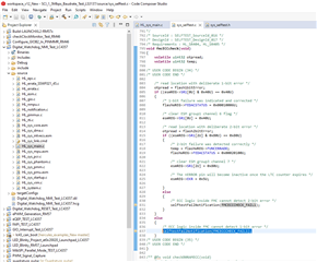
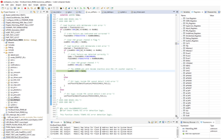
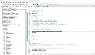
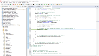
After setting RESET1(bit 15) in System Exception Control Register (SYSECR)—causing a system software reset—the MCU initialization `FMCECCCHECK_FAIL1` test is failing—which tests for successful correction of a 1-bit error on flash.
Is this behaviour expected?
Thanks for your time and support.
With my best regards,
Luis