This thread has been locked.

If you have a related question, please click the "Ask a related question" button in the top right corner. The newly created question will be automatically linked to this question.

MCU-PLUS-SDK-AM243X: Flash QSPI Deinitialisation - Undefined signals on Power Down

Part Number: MCU-PLUS-SDK-AM243X
Other Parts Discussed in Thread: AM2432

Dear TI Experts,

we are currently struggling with the power down sequence of the flash chip on our custom board with a AM2432 chip.

We activated the VMON/VSYS Monitoring to inhibit QSPI access to our external Flash Chip (ISSI IS25LP256D-RHLE).

In the attached Oscilloscope screenshot you  can observe the detection of low voltage via VMON/VSYS  on Channel 4 (by switching on a GPIO in the ISR).

As you can see on the picture, chip select is active during the power down sequence after the SW has stopped execution (GPIOs released, etc.)

Not only chip select is active, but also data is transmitted to the flash via QSPI (Please also note that these picture were made with different settings, therefore they are not 100% identical/conistent):


We are already executing the "OSPI Close" functionality in our Flash driver, but still it seems there is something remaining in a buffer and sent after the SW execution has stopped? 
Are there additional measure we can take to avoid this behavior?

We are quite sure this is causing our flash corruption issues, as it is not allowed to access the flash chip with such low voltage conditions. 

Please let me know if you need further information here.

Thanks and best regards

Robin

  • Hi Robin,

    We currently have limited bandwidth so it might take some time to come with a solution. I will be looking into your issue but please allow until next week Tuesday to receive a follow up. I will let you know. In the meantime, I would like to ask some questions:

    • Are you observing this phenomena while running an example from our API or some other code? 
      • which version of the SDK are you using?
    • Can you also share the measurement setup details (scope model, acquisition bandwidth, trigger setup, analog vs digital probes and their model numbers)

    Best,

    Daniel

  • Hi Daniel,

    thanks for your response, Robin is out of office - so I will fetch your question:

    1. We use sdk 09.00.00.05 - but our flash driver is customized based on sdk version 08.04. The application is our custom application.

    2. The oscilloscope data:
    * Rhode & Schwarz RTB2004 - 300 MHz
    * Analog Probe 10:1 (R&S RT-ZP03)
    * Trigger setup: We trigger the falling edge of the Flash Reset TP128 - see attachment (Power down sequence) Trigger level: 2.5 VDC - VCC supply flash: 3.3 VDC


    As said - we assume a issue triggered by the OSPI Hardware after application software stopped. If you need further information let us know.

    Best regards,
    Tommy
    ...

  • Hi Tommy,

    Thanks for the information, is it also possible to attach a snippet of the schematic showing the connections between the SoC and Flash device?

    Best,

    Daniel

  • Hello Daniel,

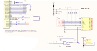
    attached you can find a larger snippet of the schematics:

    Do you need further information from our side? 

    Thanks and best regards
    Robin

  • Hello Robin,

    • To be clear, the system is designed such that when the VMON_VSYS flags under voltage then the ISR triggers OSPI0_RESET_OUT1? If this is not the case, could you please explain further how the VMON_VSYS is driving the reset operation of the OSPI device? 
      • Could you please provide additional details on how the program/ISR is setup to trigger the reset output? 
    • Can you confirm that the Dedicated RESET# Disable bit is cleared for the Dedicated RESET# to be enabled? Additional information available on the device datasheet (table 6.6)

    Regards,

    Erik

  • Hello Erik,

    1. We are not using VMON_VSYS to set the OPSI RST, the OSPI Reset is set by an additional HW voltage monitor, which pulls the OSPI Reset line if VCC drops under a certain level (about 2.9 V).
      This external HW circuit is not visible on the provided schematics.
    2. Is the second question here still relevant if the reset is not controlled by the VMON_VSYS Interrupt? Can you guide me, which datasheet/table you exactly mean? 

    The HW circuit was introduced, as set pin levels set by the SW are not applied anymore after it has stopped execution. 

    As mentioned in the initial post, we see signals on the CS and the datalines, after the SW has stopped execution and the pins are "released" from an application point of view. At least that is our understanding of the measured signals.

    Best Regards
    Robin

  • Hello Robin,

    We are not using VMON_VSYS to set the OPSI RST, the OSPI Reset is set by an additional HW voltage monitor, which pulls the OSPI Reset line if VCC drops under a certain level (about 2.9 V).
    This external HW circuit is not visible on the provided schematics.

    So the external circuit controls a reset line that goes to an AND gate to control the "NOR_RESET" signal, is that correct?

    Is the second question here still relevant if the reset is not controlled by the VMON_VSYS Interrupt? Can you guide me, which datasheet/table you exactly mean? 

    The datasheet for the ISSI device is located here.

    Table 6.6 on page 19 shows the register bit definitions. Can you please confirm through a read that Functional register bit 0 is 0 to indicate that Dedicated RESET# was enabled?

    As mentioned in the initial post, we see signals on the CS and the datalines, after the SW has stopped execution and the pins are "released" from an application point of view. At least that is our understanding of the measured signals.

    referencing the datasheet, if the the RESET# line driven low then the memory enters reset mode and output is High-Z and so any data transfers while in reset mode should not corrupt the memory. The datasheet also mentions that If RESET# is driven LOW while an internal WRITE, PROGRAM, or ERASE operation is in progress, data may be lost.

    Can you please elaborate on how you know that software has stopped execution? Is there anything that may be causing a flash read or write?

    Regards,

    Erik

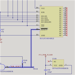
  • So the external circuit controls a reset line that goes to an AND gate to control the "NOR_RESET" signal, is that correct?

         Exactly yes, here is a snippet of the circuit:


    Can you please confirm through a read that Functional register bit 0 is 0 to indicate that Dedicated RESET# was enabled?
        Yes the value is 0, we are not using the hold/reset functionality.

    Can you please elaborate on how you know that software has stopped execution?
        
    In the first osci measurement, the position marked with "CS active during shutdown" is the point were we assume, the SW can not control the behavior of the Pins/Pads anymore. At this point the voltage levels begin to float according to there hw levels. 
    Is this assumption correct?

    We also did further tests were we tried to influence the behavior of the pads during shutdown, those tests showed us similar results.

    Is there anything that may be causing a flash read or write?
        On the measurements above, there are no intended actions to the flash, as soon as Vmon/Vsys was detected. Are there any buffer/register in UDMA, OSPI that should deinitialized before shutting  down? 
    We have no explanation for the signals visible during shutdown, they are not an intended access to the flash. 
        

  • Hello Robin,

    Can you confirm that only one data line is sending data? Can you send a screenshot of all four data lines and then if only one bus is sending data, can you please provide a screenshot of that bus, the QSPI clock, and the RESET line? This way we can decipher what command is being sent from the QSPI controller to the device.

    Are you using STIG to send commands to the flash? Is there any opcode value in the OSPI_DEV_INSTR_WR_CONFIG_REG (0x0FC40008) register by the time that you power down the device? 

    Can you confirm that this behavior directly causes flash corruption?

    Regards,

    Erik

  • Hello Erik,

    thank you for you immediate repsonse.

    Our HW Team has made some adaptions, now the mentioned hardware voltage detection is triggering the Reset Input of the AM243x. By this adaption, we don't see any further signals on the chip select, after the reset. 

    Our first attempt aimed to facilitate the Vmon Vsys functionality SW wise. We will run further tests and check the next steps depending on the results. 

    I have not checked yet the content of the  OSPI_DEV_INSTR_WR_CONFIG_REG (0x0FC40008) register. Are there general recommendations regarding this register? 

    Can you confirm that this behavior directly causes flash corruption?

    We need to run further tests, as the behavior only apears after endurance tests that run for example for one night.