This thread has been locked.

If you have a related question, please click the "Ask a related question" button in the top right corner. The newly created question will be automatically linked to this question.

AM2632-Q1: Regarding the land dimension of the IC package.

Part Number: AM2632-Q1

Hello,Expert.

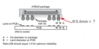
Please tell me the tolerance of the land size on the IC package side.
I want to confirm whether the land size of our printed circuit board is the same dimension as the IC package side, including tolerance, or if it is a close value.

Kind regards,

Yu Sato

  • Hi,

    Please expect a delayed response since the experts are out of office because of holidays.

    Regards,

    Shaunak

  • Hi Yu Sato,

    We recommend the land(Solder pad) size for the PCB in the Example Board layout Page (https://www.ti.com/lit/ml/mpbga29a/mpbga29a.pdf) in package details document of AM263x. That will give the details of the Solder pad size details recommended for AM263x. The same document further also has the Solder paste size recommendations.

    This document can be found by clicking on the above link or the NFBGA(ZCZ) link in the CAD/CAE Symbols section of the AM263x product page.

    Hope this answers your query.

    Thanks,

    Tejas Kulakarni

  • Hello Tejas,

    I aooreciate your prompt response.

    We read the application note SPRAA99C and wanted to verify this.

    We want to check whether the balance of the solder ball is not disturbed in the combination of the plus side of the solder pad diameter tolerance of our PCB and the minus side of the solder pad diameter tolerance of the IC package side (or in the reverse combination).

    Regards,

    Yu Sato

  • Hi Yu Sato,

    Please provide us some time to get details regarding this. I may have an answer in the next week.

    Thanks,
    Tejas Kulakarni

  • Hi,

    This image in the AM263x Datasheet shows the BGA solder ball size, which is defined as between 0.45 and 0.55 mm:

    The next page in the datasheet shows the PCB side pad arrangement and includes the recommended pad size and soldermask opening:

    The preference is to do a non-solder mask defined pad of 0.4mm with 0.5mm opening in the soldermask.  This allows the solder to flow down around the side of pad on the PCB, making for better physical adherence between the solder and the pad.

    We do not specify the package side pad size in the datasheet, but for AM263, the soldermask opening is 0.45mm.  While the pad is slightly larger on the package, this is somewhat offset by the PCB pad being non-solder mask defined as the solder flows around the side of the PCB pad.  Even still, the ratio of pad sizes is 0.4mm to 0.45mm, which is ~0.89, which is still pretty close to 1, as recommended by the SPRAA99 app note you referenced.

    Thanks,
    Mike

  • Hi,

    I updated my previous post with a correction that the first image shown is actually the solder ball size and not the package pad size.  The package pad size on AM263 is 0.45mm.

    Thanks,
    Mike