This thread has been locked.

If you have a related question, please click the "Ask a related question" button in the top right corner. The newly created question will be automatically linked to this question.

TM4C123GH6PM: New Chip

Part Number: TM4C123GH6PM
Other Parts Discussed in Thread: EK-TM4C123GXL

Hello,

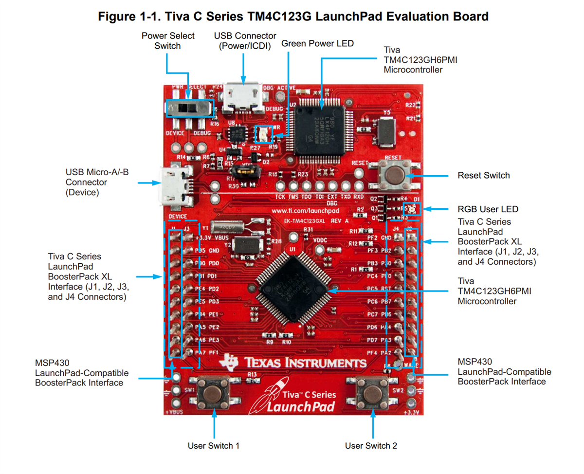
I had a question about the TM4C123, I know I have asked a similar question before, but i want to get a little more clarification about this topic. Let's say i purchase a standalone TM4C from either TI directly or an independent supplier and i want to program it with my algorithm. In addition I use the Ek-TM4C123XL Stellaris to program/debug the new chip. What would i need to connect to in the XL device and the new chip? 

(assuming I am using USB Connector (Power/ICDI) to program the new chip_

Would I use the through hole TXD & RXD (right above the white line) and the Jumper VDD?

Also, would i need to load the need chip with something in specific, maybe a bootloader program? Or just loading it with my algorithm would be sufficient?

Thank you very much for any info you all can give me. 

I want to expand the use of the MCU. 

  • Hi,

    In addition I use the Ek-TM4C123XL Stellaris to program/debug the new chip. What would i need to connect to in the XL device and the new chip? 

    There is instructions on how to use the EK-TM4C123GXL LaunchPad to debug/program another chip in section 4.6 of this app note. https://www.ti.com/lit/pdf/spma075

    Also, would i need to load the need chip with something in specific, maybe a bootloader program? Or just loading it with my algorithm would be sufficient?

    You don't need a bootloader to load your program unless you have a desire to upgrade your firmware via a communication port (e.g. SPI, UART, I2C, CAN, USB) in the future. Otherwise, you just load your firmware to 0x0. After reset or power cycle, the processor will start at 0x0 and run your program. 

  • Thank you Charles, I didn't have that document. It is definitely going to help me. 

    I was reading through SPMA075, so all i would have to do is connect the Launchpad pin TCK to pin 52 (PC0), etc..... and the Rest (right above RXD on demo board) to pin 38 RST? (plus VDD)

    Also, once i have my firmware ready to go, do i need to specify register 0x00 somehow or will it automatically start at that address. 

    I am using CCS IDE for my projects. 

  • I was reading through SPMA075, so all i would have to do is connect the Launchpad pin TCK to pin 52 (PC0), etc..... and the Rest (right above RXD on demo board) to pin 38 RST? (plus VDD)

    Yes.

    Although using a LaunchPad to debug/program another board is feasible, I will suggest you also consider a standalone low cost debug probe like XDS110 or XDS200 which is a more reliable method of debugging and developing your software. This is what I always recommend customers. The choice is yours. 

    Also, once i have my firmware ready to go, do i need to specify register 0x00 somehow or will it automatically start at that address. 

    The processor always starts from 0x0. If you load a simple program like the blinky or hello, it resides at 0x0 and the processor will fetch the stack pointer at 0x0 and then jump to your application entry point per your reset vector residing at 0x4. Your own algorithm is no different. If you are going to use a bootloader then you would need to specify a non-zero address for your application. The bootloader will reside at 0x0. Your application will reside at somewhere else like 0x2800. Until you have in mind to use bootloader, you don't need to worry about the new application address. You just build your code to start 0x0 and load it and run. 

  • Thank you very much for your help. All this information is very helpful and will apply it to my projects. 

  • Charles,

    To power the TM4C123,  should any of the VDD pins (11, 26, 42, 54) be the one to accept the 5V? If not, would it be VBAT? (what is the difference between VDD & VBAT?)

  • should any of the VDD pins (11, 26, 42, 54) be the one to accept the 5V?

    The VDD pins can only accept 3V. See the datasheet. 

    VBAT is when you want to power the device through a battery  which is also 3V supply when the the device operates on hibernate mode. Datasheet has all the detail. 

    If you have no intention to use Vbat then refer to the below diagram. There are a few more recommended block diagrams in the datasheet depending on your application requirements.