Hello!
I have a problem when sampling the voltages coming from a temperature sensor, the ADC obtains different data for each "step" of the ADC.
I have an NTC thermistor fitted into a voltage divider, the divider is powered with a voltage of 3.3V, and a fixed resistor of 3.9 kilo ohms,
the fixed resistor is the one that goes to ground. The output of this voltage divider enters an operational amplifier in follower configuration
to reduce the effects of loading, the output of the operational amplifier enters a multiplexer, and the output of the multiplexer enters the
ADC pin of the microcontroller.
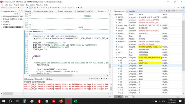
I debug the program to observe what the temperature and resistance of the sensor are like at all times. For testing purposes I replaced the
thermistor with resistors of fixed values, the voltages measured on the PCB are those expected according to the value of the resistance,
but the temperature in the code composer is not what corresponds to that resistance value, varying even by 10 degrees Celsius above the theoretical value.
Could you give me any suggestions?
void MUX_GPIO() //CONFIGURA LOS CANALES DE ADC PARA CADA COMBINACIÓN DE LOS MULTIPLEXORES
{
//CANAL 0 DEL ADC
GPIOPinWrite(GPIO_PORTE_BASE, GPIO_PIN_0, 0x00);//ENABLE1 del primer multiplexor NEGADA EN INTEGRADO
/*
//entrada S3
GPIOPinWrite(GPIO_PORTD_BASE, GPIO_PIN_5, 0xFF);//IN2
GPIOPinWrite(GPIO_PORTD_BASE, GPIO_PIN_4, 0x00);//IN1
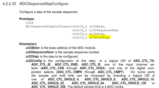
ADCSequenceConfigure(ADC0_BASE, 0, ADC_TRIGGER_PROCESSOR,0);
ADCSequenceStepConfigure(ADC0_BASE, 0,0, 0);//(paso 1)
ADCSequenceStepConfigure(ADC0_BASE, 0,1, 0);//(paso 2)
ADCSequenceStepConfigure(ADC0_BASE, 0,2, 0);//(paso 3)
ADCSequenceStepConfigure(ADC0_BASE, 0,3, 0);//(paso 4)
ADCSequenceStepConfigure(ADC0_BASE, 0,4, 0);//(paso 5)
ADCSequenceStepConfigure(ADC0_BASE, 0,5, 0);//(paso 6)
ADCSequenceStepConfigure(ADC0_BASE, 0,6, 0);//(paso 7)
ADCSequenceStepConfigure(ADC0_BASE, 0,7, 0|ADC_CTL_IE|ADC_CTL_END);//(paso 8)
ADCSequenceEnable(ADC0_BASE,0);
ADCIntClear(ADC0_BASE,0); //limpia las banderas de interrupción del ADC
ADCProcessorTrigger(ADC0_BASE,0); //Causa un trigger para una secuencia de muestreo
while(!ADCIntStatus(ADC0_BASE,0,false)) //indica el estado de las interrupciones
{
}
ADCSequenceDataGet(ADC0_BASE,0,buffer_ADC);//obtiene los datos capturados por el adc
mu_T=(buffer_ADC[0]+buffer_ADC[1]+buffer_ADC[2]+buffer_ADC[3]+buffer_ADC[4]+buffer_ADC[5]+buffer_ADC[6]+buffer_ADC[7])/8;
vol_T=mu_T*3.3/4096; //aqui hubo breakpoint
RT=((3900*(3.3-vol_T))/vol_T);
T=(1/(0.000634544+(0.000321866*log(RT))+(-0.000000306*pow(log(RT),3))))-273.15;//aqui hubo breakpoint
arreglo[2]=T;*/
//entrada S4
GPIOPinWrite(GPIO_PORTD_BASE, GPIO_PIN_5, 0xFF);//IN2
GPIOPinWrite(GPIO_PORTD_BASE, GPIO_PIN_4, 0xFF);//IN1
ADCSequenceConfigure(ADC0_BASE, 0, ADC_TRIGGER_PROCESSOR,0);
ADCSequenceStepConfigure(ADC0_BASE, 0,0, 0);//(paso 1)
ADCSequenceStepConfigure(ADC0_BASE, 0,1, 0);//(paso 2)
ADCSequenceStepConfigure(ADC0_BASE, 0,2, 0);//(paso 3)
ADCSequenceStepConfigure(ADC0_BASE, 0,3, 0);//(paso 4)
ADCSequenceStepConfigure(ADC0_BASE, 0,4, 0);//(paso 5)
ADCSequenceStepConfigure(ADC0_BASE, 0,5, 0);//(paso 6)
ADCSequenceStepConfigure(ADC0_BASE, 0,6, 0);//(paso 7)
ADCSequenceStepConfigure(ADC0_BASE, 0,7, 0|ADC_CTL_IE|ADC_CTL_END);//(paso 8)
ADCSequenceEnable(ADC0_BASE,0);
ADCIntClear(ADC0_BASE,0); //limpia las banderas de interrupción del ADC
ADCProcessorTrigger(ADC0_BASE,0); //Causa un trigger para una secuencia de muestreo
while(!ADCIntStatus(ADC0_BASE,0,false)) //indica el estado de las interrupciones
{
}
ADCSequenceDataGet(ADC0_BASE,0,buffer_ADC);//obtiene los datos capturados por el adc
mu_T=(buffer_ADC[0]+buffer_ADC[1]+buffer_ADC[2]+buffer_ADC[3]+buffer_ADC[4]+buffer_ADC[5]+buffer_ADC[6]+buffer_ADC[7])/8;
vol_T=mu_T*3.3/4096; //aqui hubo breakpoint
RT=((3900*(3.3-vol_T))/vol_T);
T=(1/(0.000634544+(0.000321866*log(RT))+(-0.000000306*pow(log(RT),3))))-273.15;//aqui hubo breakpoint
arreglo[3]=T;
//--------------------------------------------------------------------------------------------------------------------------------
}
This is my code

Mayra