This thread has been locked.

If you have a related question, please click the "Ask a related question" button in the top right corner. The newly created question will be automatically linked to this question.

MCU-PLUS-SDK-AM263X: ADC multi-channel, multi-frame DMA PaRAM Set

Part Number: MCU-PLUS-SDK-AM263X
Other Parts Discussed in Thread: SYSCONFIG

Note: This post is related to the prior thread.

  MCU-PLUS-SDK-AM263X: Continuous sampling of multiple ADCs to DMA buffers

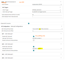
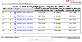
I am using EDMA to transfer ADC values from all channels of modules as seen in this diagram:


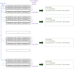
Intermittently, I see what seem to be invalid (zero) values in the destination buffer.

I need the Param Set values that I am using validated. What values (marked ?)  should I be using?

EDMA Channel PaRAM Set Entry Fields

Channel Options Parameter (OPT)     :   (EDMA_OPT_TCINTEN_MASK |
                                        ((((uint32_t)tcc) << EDMA_OPT_TCC_SHIFT) & EDMA_OPT_TCC_MASK));
                                                
Channel Source Address (SRC)        :   (uint32_t) SOC_virtToPhy((void *)(adc_base+CSL_ADC_RESULT_ADCRESULT0));

Channel Destination Address (DST)   :   (uint32_t) SOC_virtToPhy((void *) dest_buf);

Count for 1st Dimension (ACNT)      :   ?

Count for 2nd Dimension (BCNT)      :   ?

Count for 3rd Dimension (CCNT)      :   ?

BCNT Reload (BCNTRLD)               :   ?

Source B Index (SBIDX)              :   ?

Destination B Index (DBIDX)         :   ?

Source C Index (SCIDX)              :   ?

Destination C Index (DCIDX)         :   ?

Link Address (LINK)                 :   0xFFFFU

  • Hi TollMan,

    Let me look into it and get back to you by tomorrow.


    Thanks and Regards

    Akshit

  • Hi,

    EDMA Channel PaRAM Set Entry Fields
    
    Channel Options Parameter (OPT)     :   (EDMA_OPT_TCINTEN_MASK |
                                            ((((uint32_t)tcc) << EDMA_OPT_TCC_SHIFT) & EDMA_OPT_TCC_MASK));
                                                    
    Channel Source Address (SRC)        :   (uint32_t) SOC_virtToPhy((void *)(adc_base+CSL_ADC_RESULT_ADCRESULT0));
    
    Channel Destination Address (DST)   :   (uint32_t) SOC_virtToPhy((void *) dest_buf);
    
    Count for 1st Dimension (ACNT)      :   (uint16_t) 2   // Number of bytes in each Array (sizeof(uint16_t))
    
    Count for 2nd Dimension (BCNT)      :   (uint16_t) 6   // Number of Arrays in each frame (Channels in this case)
    
    Count for 3rd Dimension (CCNT)      :   (uint16_t) 256 // Number of Frames in a block (or number of transfers here -> 256)
    
    BCNT Reload (BCNTRLD)               :   0	           // Don't need for AB-Sync; for A-sync When BCNT reaches 0, the EDMA_TPCC decrements CCNT and uses the BCNTRLD value to reinitialize the BCNT value.
    
    Source B Index (SBIDX)              :   EDMA_PARAM_BIDX(CSL_ADC_RESULT_ADCRESULT1 - CSL_ADC_RESULT_ADCRESULT0); // byte address offset between start index of ADC0 and ADC1 channels (Arrays in the same frame)
    
    Destination B Index (DBIDX)         :   EDMA_PARAM_BIDX(CSL_ADC_RESULT_ADCRESULT1 - CSL_ADC_RESULT_ADCRESULT0); // byte address offset between beginning of destination array to the beginning of the next destination array in the same frame
    
    Source C Index (SCIDX)              :   EDMA_PARAM_BIDX(0)  // byte address offset from the beginning of the current array (pointed to by SRC address) to the beginning of the first source array in the next frame (0 in this case)
    
    Destination C Index (DCIDX)         :   EDMA_PARAM_BIDX(CSL_ADC_RESULT_ADCRESULT5 - CSL_ADC_RESULT_ADCRESULT0)  // byte address offset from the beginning of the current array (pointed to by DST address) to the beginning of the first destination array TR in the next frame. (diff b'w adc_res5 and adc_res0 )
    
    Link Address (LINK)                 :   0xFFFFU

    Please refer to TRM section 11.2.3.3.2 for more information.
    Regards,
    Akshit
  • The parameter set values make sense based on the reference manual descriptions, however, there is something wrong.


    This is how I am testing.


    1)

    Start with SDK example:

      adc_soc_continuous_dma_am263px-cc_r5fss0-0_nortos_ti-arm-clang


    2)

    Modify SysConfig to:

    • Add SOCs for each ADC channel. Six total channels per module.
    • Make EPWM20 the sampling time base to have a configurable sample frequency based on EPWM period.
    • Make all SOC Triggers from EPWM20. No INT1 trigger for ‘continuous mode’.
    • Make All priorities are based on SOC number
    • Make ADC INT2 trigger is SOC5. The last channel.
      • After SOC5 all channels are ready to transfer.

    3)

    Modify adc_soc_continuous_dma.c to:

    • Increase buffer size for the additional channels.
    • Remove ADC1 code to disable PWM SOC trigger.
    • Reduce DMA transfer number to 256.
    • Change printf to print all samples for all channels.
    • Use the suggested Param Set parameters.


    Results:


    The beginning and end of the printfs look like this:


    [Cortex_R5_0] ADC Continuous DMA transfer Test Started ...

    ADC1 : ADC2 Result register value -

    4095,4095,555,2602,3961,3921:1535,2600,562,2605,1,1

    0,0,0,0,0,0:0,0,0,0,0,0

    0,0,0,0,0,0:0,0,0,0,0,0

    0,0,0,0,0,0:0,0,0,0,0,0

    ADC Continuous DMA transfer Test Passed

    All tests have passed!!

    All intermediate values (excluded) are zero.


    Observations:

    • Some of the first SOCs for ADC2 (1535, 562) make sense, but none of the other values do.
    • If I poll the ADC, the values are correct. This is not a hardware setup issue.

    I also checked the buffer with the debugger to make sure there isn't a printf() issue. The values in the buffer match the printf. 

    I am attaching my project.


    adc_soc_epwm_multi_dma_am263px-cc_p02.zip

    Why are the ADC samples bad?


    Regards,

    Tollman

  • Hi Tollman, 

    I was checking through your project. the thread mentions it is a AM263x, whereas project is on AM263Px. anyways, the behavior might be similar.

    Can we get on a call to quickly discuss and close this? 

    thanks and regards,

    Madhava

  • Hello Madhava,  (I'm jumping in here if I may to help potentially coordinate a call as you suggested)

    Our customer is located in Dallas area/CST time and we realize you are Bangalore time.  (I am EST)

    For today 03/26/2024, customer is available:

    Availability starts: 09:00am CST

    Not Available: 10:00-11:30

    Not Available: 14:00-15:30

    Availability Ends: 20:00pm CST

     Could you squeeze in a half-hour sometime today?

    Thank you,

    Chris 

  • Hi Scott, 

    to Summarize the call,

    1. have an extra, SOC towards the end, that has same trigger as all the actual ones. Configure INT to the last SOC to trigger DMA.
    2. remove the empty channel transfer,
    3. configure DMA channel to have AB sync transfer (refer to link or chain transfer examples of edma)

    Also, Thanks Chris for quick call setup!

    thanks and regards,

    Madhava

  • Hi Madhava,

    I made the recommended changes, but there is still a problem. I think my Param Set still has a problem.

    These are the changes I made inline with your recommend changes.

    1. have an extra, SOC towards the end, that has same trigger as all the actual ones. Configure INT to the last SOC to trigger DMA.

    See sysconfig screen capture here:

    2. remove the empty channel transfer,

    I removed the empty transfer configuration from App_dmaConfigure()

    3. configure DMA channel to have AB sync transfer (refer to link or chain transfer examples of edma)

    I tried to adjust the param set based on our discussion. 

    a. Add the EDMA_OPT_SYNCDIM_MASK to opt for AB transfer.

    b. Account for the offset between SOC result registers.

    However, if I read the register addendum correctly, I think the offset should be 2 bytes. I think this is different than we discussed. Correct?

    After trying a few things, I decided to post the current project here for review.

    adc_soc_epwm_multi_dma_am263px-cc_p02(2).zip

    The printfs look like:

    [Cortex_R5_0] ADC Continuous DMA transfer Test Started ...
    ADC1 : ADC2 Result register value -
    4095,4095,554,4095,4095,4095:0,0,0,0,0,0
    4095,4095,554,4095,4095,4081:0,0,0,0,0,0
    4095,4063,555,4095,4059,4002:0,0,0,0,0,0
    4064,4015,555,4095,4010,3926:0,0,0,0,0,0
    4016,3967,555,4076,3961,3852:0,0,0,0,0,0
    3968,3919,555,4049,3914,3778:0,0,0,0,0,0
    3921,3873,557,4021,3867,3707:0,0,0,0,0,0

    ...

    1527,1516,556,1661,1516,1664:0,0,0,0,0,0
    1527,1515,555,1657,1515,1663:0,0,0,0,0,0
    1526,1515,556,1656,1515,1663:0,0,0,0,0,0
    ADC Continuous DMA transfer Test Passed
    All tests have passed!!

    Please review.

    Thanks,

    Tollman

  • Hi Scott, 

    Apologies for the delayed response. 

    However, if I read the register addendum correctly, I think the offset should be 2 bytes. I think this is different than we discussed. Correct?

    Yes the ADC results are 16 bit and are offset by 2 bytes. thanks for pointing.

    I checked your application code, you have used the 2 byte offsets. this seems fine. Are your results matching your inputs? 

    thanks and regards,

    Madhava

  • Hi Madhava

    As seen in the printfs above, ADC2 is not updating the DMA buffer. I compared with projects with successful transfers with more than one ADC module, but I do not see the discrepancy.

    What I am about to post below is a brief overview of the contents of the pdf I am attaching. I spent a lot of time formatting that document to make the issue as clear as possible. Replicating than formatting in this UI would be tedious.

    I am also attaching the project that I archived while configured for Test Case 4.

    MCU-PLUS-SDK-AM263X- ADC multi-channel, multi-frame DMA PaRAM Set.pdf

    adc_soc_epwm_multi_dma_am263px-cc_p02(3).zip

    Here I s the summary:


    Discovery: DMA Configuration Order

    DMA Configuration, Order determines which ADC module has transfers.

    The DMA configured first has transfers with value ADC values..


    Changes to project attached to previous post:

    • Initialize all buffers to default values exceeding the ADC range.


    Analysis:

    • (I think) This suggests that the ADC configuration for both modules is valid.
    • (I think) This suggests that the DMA_TRIGGER, and DMA_XBAR configuration for both modules are valid.


    Observations:

    • ADC_RESULT registers always hold valid values.


    Questions:

    • Is using the same SOC trigger for all ADCs (ePWM20, ADCSOCA)? IS there a maximum ‘fan-out’?
    • Is there a problem in the channel or event queue configuration (based on the continuous DMA SDK example (also using two modules)) that is affecting this project?

    Regards,

    Scott

  • Hi Scott, 

    I checked your pdf. its very detailed and points the one thing we missed discussing in the call. your syscfg configurations are configuring the ADC2_INT2 to trigger the DMA channel 2, where as the code is line # 276 is trying to allocate the readily available channel (which will be DMA Channel 1 in this case).

    Could you please try commenting out the line # 276 to 278 and see if it resolves the issue on the ADC 2 results transfer? here essentially what we are doing is we are allocating the DMA Channel, passed as argument to the function.  

  • I make the suggested change. Which was to remove the call to:

       EDMA_allocDmaChannel()

    inside

      App_dmaConfigure()

    .


    Additionaly I had to modify the calls to funtions:

      EDMA_configureChannelRegion()

      EDMA_enableTransferRegion()

    …to use the argument

      uint32_t dma_ch

    … passed to

      App_dmaConfigure()

    .


    Now, upon initial inspection, the print looks good:


    [Cortex_R5_0] ADC Continuous DMA transfer Test Started ...

    ADC1 : ADC2 Result register value -

    2494,4095,543,2507,4095,4095:1513,3206,554,2501,0,1

    2514,4095,550,2513,4095,4081:1538,2603,557,2510,1,1

    2523,4061,555,2522,4059,4002:1549,2213,561,2518,0,1

    2530,4013,555,2530,4010,3926:1549,1961,561,2527,1,2

    2536,3964,551,2538,3961,3852:1539,1797,559,2534,0,1

    2544,3918,547,2545,3914,3778:1526,1691,553,2541,1,1

    2553,3872,552,2553,3867,3707:1542,1625,559,2549,1,1

    2562,3827,555,2562,3822,3639:1548,1582,562,2558,0,2

    2570,3782,554,2571,3777,3574:1548,1552,563,2566,1,1

    2578,3739,549,2577,3733,3513:1532,1531,556,2573,0,1

    2585,3697,546,2585,3690,3456:1528,1519,554,2581,0,1

    2593,3656,551,2592,3648,3399:1541,1513,559,2589,0,2

    2602,3616,555,2603,3607,3345:1550,1509,562,2597,0,1

    2610,3576,555,2609,3566,3290:1549,1504,561,2605,1,1

    2616,3537,552,2615,3526,3237:1543,1501,559,2611,1,1

    2622,3498,547,2621,3488,3185:1527,1498,554,2618,0,1

    2629,3462,548,2629,3450,3137:1532,1499,555,2625,1,1

    2637,3424,554,2636,3412,3089:1547,1499,561,2631,0,1

    2643,3388,556,2642,3376,3047:1550,1499,563,2638,1,1

    . . .

    2614,1528,556,2614,1523,1663:1549,1497,561,2610,0,2

    2607,1526,555,2607,1523,1663:1548,1496,561,2603,1,1

    2601,1527,552,2599,1523,1664:1539,1495,558,2596,0,2

    2592,1526,546,2590,1522,1663:1524,1494,552,2587,0,1

    2584,1526,553,2583,1521,1663:1540,1496,557,2580,1,1

    2576,1525,555,2575,1521,1663:1551,1497,562,2572,0,1

    2570,1526,555,2568,1521,1663:1548,1497,561,2564,0,1

    ADC Continuous DMA transfer Test Passed

    All tests have passed!!


    I may have a follow-up question about why the adc_soc_continuous_dma_am263px-cc_r5fss0-0_nortos_ti-arm-clang SDK example may allocate DMA similar what was fixed in my code.

    I consider this thread resolved.