This thread has been locked.

If you have a related question, please click the "Ask a related question" button in the top right corner. The newly created question will be automatically linked to this question.

AM2634-Q1: ADC input model and Sampling Window config

Part Number: AM2634-Q1

Hello,

can you please direct me to where I can find the ADC input model for AM2634COKFHMZCZRQ1. It's mentioned on the reference manual that the values can be found on the datasheets, but I couldn't locate it.

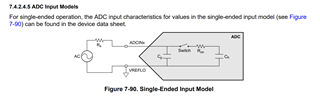
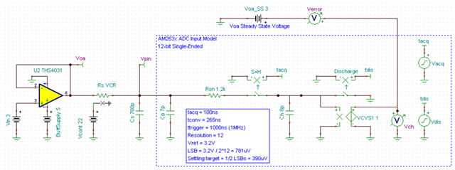
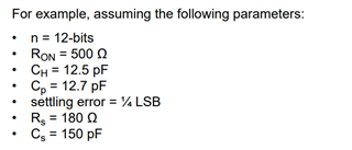
Should I use the Ron and Ch values used in the example given in page 491 of the reference manual ?

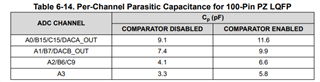
can you provide the table for the pin capacitance for each of the analogue inputs ?

Thanks,

Yassine

  • Hello Yassine,

    We are working to get a TINA ADC Input Model provided on the product page. In the meantime, please use the information below to get started.

    n = 12 bits

    Ron = 1.2k

    C= 8pF

    C= 7pF

    Settling Error = 1/2 LSB 

    Rs = Calculate

    Cs = 700pF

    The pin capacitance for each ADC pin is Ch||Cp

    = 15pF

    Best Regards,

    Zackary Fleenor

  • Thanks Zackary for the feedback.

    do all pins have the same parasitic cap ? you have a table like the following for the AM263x : 

    regarding the VREFHI pins connection when using internal reference mode, can you please elaborate on the following

    AM2634-Q1: Sysconfig enables internal reference by default and ADC_VREFHI_G0/G1 should not connect to ADC_VREFHI_G2 directly?

    what kind of damage/conflict should I expect ?

    Thanks again,

    Yassine

  • Hello Yassine,

    Yes, All ADC Input pins have the same parasitic capacitor. We do not have a table like the one shown as it is not relevant for the AM263x ADC design.

    If you connect ADC_VREFHI_G[0:2] directly and use the internal reference mode, at the least, it will likely burn out the ADC reference circuitry completing rendering the ADC's useless, a worse case is that the AnalogCIO/Power Mangement Unit is damaged resulting in a completely bricked device.

    Best Regards,

    Zackary Fleenor

  • Thanks Zackary,

    Regarding the ADC total unadjusted error. are ,max/min the values shown in the datasheet correspond only to the the internal reference mode tolerances ? What to expect for more precise external reference ? 

    I'm using the following formula to calculate the TUE.

    Can you please elaborate how to take into account the inter-channels errors ? are they related to cross-talk ? could those errors be avoided ?

    Thanks,

    Yassine

  • Hello Yassine,

    I have reached out to the design expert here to provide some additional information. Please allow up to two days for them to review and respond.

    Best Regards,

    Zackary Fleenor

  • Apologies for the delayed response here. I have pinged our design engineer to provide some additional information as soon as possible.

    Best Regards,

    Zackary Fleenor

  • Hi Zackary,

    Any feedback on the above inquiry ?

    Thanks

  • Hello Yassine,

    Design team had the following feedback:

    1) An improved external reference voltage should help to reduce gain error.

    2) For inter-channel errors - It's not just crosstalk, but possible difference in the channel paths for the ADC. In particular, odd channels and even channels have different internal signal paths that can cause differences in those channels. This won't be avoidable due to the fact that it's innately embedded in the ADC analog design. The variability between the various channel paths could be logged over time and accounted for as part of the application code.

    Best Regards,

    Zackary Fleenor