Part Number: AM2631
Tool/software:
Hello,
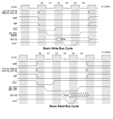
Strongly based on the SDK's GPMC sample code, the GPMC module was set for synchronous communication (at 21.33MHz -192MHz/9-) looking for the following behavior on a write cycle (RE-Rising edge, FE-Falling edge):
RE0: BE1 low, Address/Data set, ADV low, WE low
FE0: CS0 low
RE1:ADV high
FE1: -
RE2: WAIT0 sampling (to be repeated if active until inactive)
FE2: CSn0 high
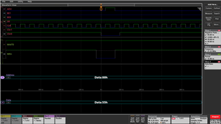
However, the WAIT0 signal seems to be ignored -for both low and high levels-, as seen in the scope (attached): waveform is the same irrespective of the WAIT0 state. Also attached is a memory dump of the GPMC registers settings.
Should another setting be changed to achieve the sampling of WAIT0 signal?
Regards,
Javier
0x48400018	00000000	00000000	00000000	00000000	00000000	00000000	00000000
0x48400034	00000000	00000000	00000000	00001FF0	484000AC	00000211	00000000
0x48400050	00000000	00000301	00000000	00000000	08601003	00020280	11010100
0x4840006C	02004280	03010202	01010001	00000F68	FFFBFFFB	FFFBFFFB	FFFBFFFB
0x48400088	00000000	00000000	00001000	00101001	22060514	10057016	010F1111
0x484000A4	8F070000	00000F00	????????	????????	????????	00000000	00000000
0x484000C0	00001000	00101001	22060514	10057016	010F1111	8F070000	00000F00
0x484000DC	????????	????????	????????	00000000	00000000	00001000	00101001
0x484000F8	22060514	10057016	010F1111	8F070000	00000F00	????????	????????
0x48400114	????????	00000000	00000000	00001000	00101001	22060514	10057016
0x48400130	010F1111	8F070000	00000F00	????????	????????	????????	00000000
0x4840014C	00000000	00001000	00101001	22060514	10057016	010F1111	8F070000
0x48400168	00000F00	????????	????????	????????	00000000	00000000	00001000
0x48400184	00101001	22060514	10057016	010F1111	8F070000	00000F00	????????
0x484001A0	????????	????????	00000000	00000000	00001000	00101001	22060514
0x484001BC	10057016	010F1111	8F070000	00000F00	????????	????????	????????
0x484001D8	00000000	00000000	00004000	00000000	00000000	00000000	00000000
0x484001F4	00001030	00000000	FFFFF000	00000000	00000000	00000000	00000000
0x48400210	00000000	00000000	00000000	00000000	00000000	00000000	00000000