This thread has been locked.

If you have a related question, please click the "Ask a related question" button in the top right corner. The newly created question will be automatically linked to this question.

MCU-PLUS-SDK-AM263X: AM2634

Part Number: MCU-PLUS-SDK-AM263X

Tool/software:

   I am using AM263X-LP and wants to implement simultaneous sampling on 4 adc channel(all channel working at its maximum sampling rate), what is best example project to refer for?

  Pls tell the difference in output obtained in two situations mentioned below

        1. implementation of simultaneous sampling using 1 adc module and utilizing it's 4 channel.

        2. implementation of simultaneous sampling using 4 adc module and utilizing single channel of each.

  • Hey Tej,

    Please refer to the ADC Multiple SOC EPWM example from the SDK.

    https://software-dl.ti.com/mcu-plus-sdk/esd/AM263X/latest/exports/docs/api_guide_am263x/EXAMPLES_DRIVERS_ADC_MULTIPLE_SOC_EPWM.html

    A single ADC will be unable to simultaneously sample 4 different sample voltages. However, you could time multiplex the sampling of 4 unique channels. Using a single channel of 4 separate ADC's would allow you to simultaneously sample 4 different signals. The output value obtained would not differ between the methods.

    Best Regards,

    Zackary Fleenor

  • Hii Fleenor,

    Thanks for your suggestions,
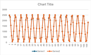
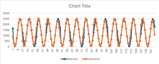
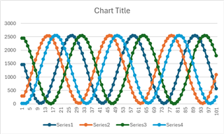
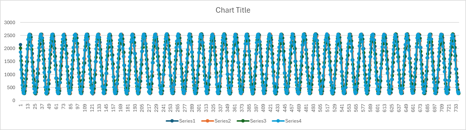
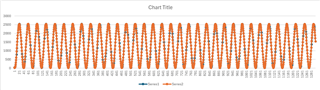
    After going through multiple thread in ti E2E, I realised AM263x MCU+ SDK: ADC SOC Continuous DMA  is better option for simultaneous sampling for higher frequency signal. it is working well when i am setting the sampling rate at 3.2 MSPS(or low) but when i set sampling rate to 4MSPS ( by changing the adc clk prescaler) there is phase difference for same signal(both signal with same properties) on both the channel. below i have attached the image for same.

    how to resolve this issue??


    sampling rate = 3.2msps(approx) , frequency of sine wave= 400KHz(on both channel)


    sampling rate = 4msps , frequency of sine wave= 400KHz(on both channel)

  • Hey Tej,

    Just to confirm our understanding:

    You are using 2 channels (Orange & Blue lines) from the same ADC?

  • No, i am using two different adc instances ADC1 and ADC2(one channel of each). 

  • Understood thanks for the clarification, and for the 400KHz sine wave, is there a dedicated source for each channel or a single source that is branched to the two input channels?

  • Hii Fleenor,

    There is dedicated source for each channel.

    I am taking sine wave from the two different channel of function generator but i am making sure these setting-

    1. phase channel 1 = phase of channel 2

    2. frequency of channel 1 = frequency of channel 2

    3. Level of channel 1 = Level of channel 2

  • Thanks for the info. A few more follow up questions:

    1) Are the connections wires directly from the function generator to the launchpad pins?

           1a) Are they the same length, gauge, and connectors? 

           1b) Are you able to test with a dedicated function generator per channel? 

    2) Have you made any modifications to the Launchpad?

    3) Can you share the project ADC configuration details?

    Best Regards.

    Zackary Fleenor

  • Hii Fleenor,

    1. I am taking ADC signal from the function generator to launchpad pins via BNC crocodile wire ( with help of male to female jumper wire ).

       1 (a) Yes, they are of same length gauge, and connectors.

       1 (b) Actually there are two channel in function generator( both are synchronized as mentioned earlier). Output of channel 1 is given to pin
                ADC1ANIN0 and channel 2 is given to pin ADC2ANIN0.

    2. Yes, i have removed the corresponding capacitor to pin ADC1ANIN0(C72), ADC1ANIN0(C73) , ADC2ANIN0 (C74) and ADC2ANIN0(C75).
         Because they were making low pass filter( recommended by you in previous thread).

    3. Since i wants to extend the example project to work for 4 ADC channel (1 channel of 4 different  ADC instance).
         But i am getting some error in that while working for 3 and 4 channel, actually it is working for 2 channels but for third channel the adc result 
    register value is not getting updated in dma buffer (it only show initial value which is 0).

        ti_driver_open_close.c


    /*
     * EDMA
     */
    /* EDMA Driver handles */
    EDMA_Handle gEdmaHandle[CONFIG_EDMA_NUM_INSTANCES];
    
    /* EDMA Driver Open Parameters */
    EDMA_Params gEdmaParams[CONFIG_EDMA_NUM_INSTANCES] =
    {
        {
            .intrEnable = TRUE,
        },
    };
    
    void Drivers_edmaOpen(void)
    {
        uint32_t instCnt;
        int32_t  status = SystemP_SUCCESS;
    
        for(instCnt = 0U; instCnt < CONFIG_EDMA_NUM_INSTANCES; instCnt++)
        {
            gEdmaHandle[instCnt] = NULL;   /* Init to NULL so that we can exit gracefully */
        }
    
        /* Open all instances */
        for(instCnt = 0U; instCnt < CONFIG_EDMA_NUM_INSTANCES; instCnt++)
        {
            gEdmaHandle[instCnt] = EDMA_open(instCnt, &gEdmaParams[instCnt]);
            if(NULL == gEdmaHandle[instCnt])
            {
                DebugP_logError("EDMA open failed for instance %d !!!\r\n", instCnt);
                status = SystemP_FAILURE;
                break;
            }
        }
    
        if(SystemP_FAILURE == status)
        {
            Drivers_edmaClose();   /* Exit gracefully */
        }
    
        return;
    }
    
    void Drivers_edmaClose(void)
    {
        uint32_t instCnt;
    
        /* Close all instances that are open */
        for(instCnt = 0U; instCnt < CONFIG_EDMA_NUM_INSTANCES; instCnt++)
        {
            if(gEdmaHandle[instCnt] != NULL)
            {
                EDMA_close(gEdmaHandle[instCnt]);
                gEdmaHandle[instCnt] = NULL;
            }
        }
    
        return;
    }
    
    void Drivers_epwmOpen(void)
    {
    	/* CONFIG_EPWM0 initialization */
    
    	/* Time Base */
    	EPWM_setEmulationMode(CONFIG_EPWM0_BASE_ADDR, EPWM_EMULATION_FREE_RUN);
    	EPWM_setClockPrescaler(CONFIG_EPWM0_BASE_ADDR, EPWM_CLOCK_DIVIDER_1, EPWM_HSCLOCK_DIVIDER_1);
    	EPWM_setTimeBasePeriod(CONFIG_EPWM0_BASE_ADDR, 1000);
    	EPWM_disableGlobalLoadRegisters(CONFIG_EPWM0_BASE_ADDR, EPWM_GL_REGISTER_TBPRD_TBPRDHR);
    	EPWM_setPeriodLoadMode(CONFIG_EPWM0_BASE_ADDR, EPWM_PERIOD_SHADOW_LOAD);
        EPWM_selectPeriodLoadEvent(CONFIG_EPWM0_BASE_ADDR, EPWM_SHADOW_LOAD_MODE_COUNTER_ZERO);
    	EPWM_setTimeBaseCounter(CONFIG_EPWM0_BASE_ADDR, 0);
    	EPWM_setTimeBaseCounterMode(CONFIG_EPWM0_BASE_ADDR, EPWM_COUNTER_MODE_STOP_FREEZE);
    	EPWM_setCountModeAfterSync(CONFIG_EPWM0_BASE_ADDR, EPWM_COUNT_MODE_DOWN_AFTER_SYNC);
    	EPWM_disablePhaseShiftLoad(CONFIG_EPWM0_BASE_ADDR);
    	EPWM_setPhaseShift(CONFIG_EPWM0_BASE_ADDR, 0);
    	EPWM_enableSyncOutPulseSource(CONFIG_EPWM0_BASE_ADDR, 0);
    	EPWM_setSyncInPulseSource(CONFIG_EPWM0_BASE_ADDR, EPWM_SYNC_IN_PULSE_SRC_DISABLE);
    	EPWM_setOneShotSyncOutTrigger(CONFIG_EPWM0_BASE_ADDR, EPWM_OSHT_SYNC_OUT_TRIG_SYNC);
    	
        HRPWM_setSyncPulseSource(CONFIG_EPWM0_BASE_ADDR, HRPWM_PWMSYNC_SOURCE_PERIOD);
    
    	/* Counter Compare */
    	EPWM_setCounterCompareValue(CONFIG_EPWM0_BASE_ADDR, EPWM_COUNTER_COMPARE_A, 499);
    	EPWM_disableGlobalLoadRegisters(CONFIG_EPWM0_BASE_ADDR, EPWM_GL_REGISTER_CMPA_CMPAHR);
    	
    	EPWM_setCounterCompareShadowLoadMode(CONFIG_EPWM0_BASE_ADDR, EPWM_COUNTER_COMPARE_A, EPWM_COMP_LOAD_ON_CNTR_ZERO);
    	EPWM_setCounterCompareValue(CONFIG_EPWM0_BASE_ADDR, EPWM_COUNTER_COMPARE_B, 0);
    	EPWM_disableGlobalLoadRegisters(CONFIG_EPWM0_BASE_ADDR, EPWM_GL_REGISTER_CMPB_CMPBHR);
    	
    	EPWM_setCounterCompareShadowLoadMode(CONFIG_EPWM0_BASE_ADDR, EPWM_COUNTER_COMPARE_B, EPWM_COMP_LOAD_ON_CNTR_ZERO);
    	EPWM_setCounterCompareValue(CONFIG_EPWM0_BASE_ADDR, EPWM_COUNTER_COMPARE_C, 0);
    	EPWM_disableGlobalLoadRegisters(CONFIG_EPWM0_BASE_ADDR, EPWM_GL_REGISTER_CMPC);
    	
    	EPWM_setCounterCompareShadowLoadMode(CONFIG_EPWM0_BASE_ADDR, EPWM_COUNTER_COMPARE_C, EPWM_COMP_LOAD_ON_CNTR_ZERO);
    	EPWM_setCounterCompareValue(CONFIG_EPWM0_BASE_ADDR, EPWM_COUNTER_COMPARE_D, 0);
    	EPWM_disableGlobalLoadRegisters(CONFIG_EPWM0_BASE_ADDR, EPWM_GL_REGISTER_CMPD);
    	
    	EPWM_setCounterCompareShadowLoadMode(CONFIG_EPWM0_BASE_ADDR, EPWM_COUNTER_COMPARE_D, EPWM_COMP_LOAD_ON_CNTR_ZERO);
    
    	/* Action Qualifier */
    	EPWM_disableGlobalLoadRegisters(CONFIG_EPWM0_BASE_ADDR, EPWM_GL_REGISTER_AQCSFRC);
    	EPWM_setActionQualifierContSWForceShadowMode(CONFIG_EPWM0_BASE_ADDR, EPWM_AQ_SW_SH_LOAD_ON_CNTR_ZERO);
    	EPWM_disableGlobalLoadRegisters(CONFIG_EPWM0_BASE_ADDR, EPWM_GL_REGISTER_AQCTLA_AQCTLA2);
    	EPWM_disableActionQualifierShadowLoadMode(CONFIG_EPWM0_BASE_ADDR, EPWM_ACTION_QUALIFIER_A);
    	EPWM_setActionQualifierShadowLoadMode(CONFIG_EPWM0_BASE_ADDR, EPWM_ACTION_QUALIFIER_A, EPWM_AQ_LOAD_ON_CNTR_ZERO);
    	EPWM_setActionQualifierT1TriggerSource(CONFIG_EPWM0_BASE_ADDR, EPWM_AQ_TRIGGER_EVENT_TRIG_DCA_1);
    	EPWM_setActionQualifierT2TriggerSource(CONFIG_EPWM0_BASE_ADDR, EPWM_AQ_TRIGGER_EVENT_TRIG_DCA_1);
    	EPWM_setActionQualifierSWAction(CONFIG_EPWM0_BASE_ADDR, EPWM_AQ_OUTPUT_A, EPWM_AQ_OUTPUT_NO_CHANGE);
    	EPWM_setActionQualifierContSWForceAction(CONFIG_EPWM0_BASE_ADDR, EPWM_AQ_OUTPUT_A, EPWM_AQ_SW_DISABLED);
    	EPWM_disableGlobalLoadRegisters(CONFIG_EPWM0_BASE_ADDR, EPWM_GL_REGISTER_AQCTLB_AQCTLB2);
    	EPWM_disableActionQualifierShadowLoadMode(CONFIG_EPWM0_BASE_ADDR, EPWM_ACTION_QUALIFIER_B);
    	EPWM_setActionQualifierShadowLoadMode(CONFIG_EPWM0_BASE_ADDR, EPWM_ACTION_QUALIFIER_B, EPWM_AQ_LOAD_ON_CNTR_ZERO);
    	EPWM_setActionQualifierSWAction(CONFIG_EPWM0_BASE_ADDR, EPWM_AQ_OUTPUT_B, EPWM_AQ_OUTPUT_NO_CHANGE);
    	EPWM_setActionQualifierContSWForceAction(CONFIG_EPWM0_BASE_ADDR, EPWM_AQ_OUTPUT_B, EPWM_AQ_SW_DISABLED);
    
    	/* Events */
    	EPWM_setActionQualifierAction(CONFIG_EPWM0_BASE_ADDR, EPWM_AQ_OUTPUT_A, EPWM_AQ_OUTPUT_HIGH, EPWM_AQ_OUTPUT_ON_TIMEBASE_ZERO);
    	EPWM_setActionQualifierAction(CONFIG_EPWM0_BASE_ADDR, EPWM_AQ_OUTPUT_A, EPWM_AQ_OUTPUT_NO_CHANGE, EPWM_AQ_OUTPUT_ON_TIMEBASE_PERIOD);
    	EPWM_setActionQualifierAction(CONFIG_EPWM0_BASE_ADDR, EPWM_AQ_OUTPUT_A, EPWM_AQ_OUTPUT_LOW, EPWM_AQ_OUTPUT_ON_TIMEBASE_UP_CMPA);
    	EPWM_setActionQualifierAction(CONFIG_EPWM0_BASE_ADDR, EPWM_AQ_OUTPUT_A, EPWM_AQ_OUTPUT_NO_CHANGE, EPWM_AQ_OUTPUT_ON_TIMEBASE_DOWN_CMPA);
    	EPWM_setActionQualifierAction(CONFIG_EPWM0_BASE_ADDR, EPWM_AQ_OUTPUT_A, EPWM_AQ_OUTPUT_NO_CHANGE, EPWM_AQ_OUTPUT_ON_TIMEBASE_UP_CMPB);
    	EPWM_setActionQualifierAction(CONFIG_EPWM0_BASE_ADDR, EPWM_AQ_OUTPUT_A, EPWM_AQ_OUTPUT_NO_CHANGE, EPWM_AQ_OUTPUT_ON_TIMEBASE_DOWN_CMPB);
    	EPWM_setActionQualifierAction(CONFIG_EPWM0_BASE_ADDR, EPWM_AQ_OUTPUT_A, EPWM_AQ_OUTPUT_NO_CHANGE, EPWM_AQ_OUTPUT_ON_T1_COUNT_UP);
    	EPWM_setActionQualifierAction(CONFIG_EPWM0_BASE_ADDR, EPWM_AQ_OUTPUT_A, EPWM_AQ_OUTPUT_NO_CHANGE, EPWM_AQ_OUTPUT_ON_T1_COUNT_DOWN);
    	EPWM_setActionQualifierAction(CONFIG_EPWM0_BASE_ADDR, EPWM_AQ_OUTPUT_A, EPWM_AQ_OUTPUT_NO_CHANGE, EPWM_AQ_OUTPUT_ON_T2_COUNT_UP);
    	EPWM_setActionQualifierAction(CONFIG_EPWM0_BASE_ADDR, EPWM_AQ_OUTPUT_A, EPWM_AQ_OUTPUT_NO_CHANGE, EPWM_AQ_OUTPUT_ON_T2_COUNT_DOWN);
    	EPWM_setActionQualifierAction(CONFIG_EPWM0_BASE_ADDR, EPWM_AQ_OUTPUT_B, EPWM_AQ_OUTPUT_NO_CHANGE, EPWM_AQ_OUTPUT_ON_TIMEBASE_ZERO);
    	EPWM_setActionQualifierAction(CONFIG_EPWM0_BASE_ADDR, EPWM_AQ_OUTPUT_B, EPWM_AQ_OUTPUT_NO_CHANGE, EPWM_AQ_OUTPUT_ON_TIMEBASE_PERIOD);
    	EPWM_setActionQualifierAction(CONFIG_EPWM0_BASE_ADDR, EPWM_AQ_OUTPUT_B, EPWM_AQ_OUTPUT_NO_CHANGE, EPWM_AQ_OUTPUT_ON_TIMEBASE_UP_CMPA);
    	EPWM_setActionQualifierAction(CONFIG_EPWM0_BASE_ADDR, EPWM_AQ_OUTPUT_B, EPWM_AQ_OUTPUT_NO_CHANGE, EPWM_AQ_OUTPUT_ON_TIMEBASE_DOWN_CMPA);
    	EPWM_setActionQualifierAction(CONFIG_EPWM0_BASE_ADDR, EPWM_AQ_OUTPUT_B, EPWM_AQ_OUTPUT_NO_CHANGE, EPWM_AQ_OUTPUT_ON_TIMEBASE_UP_CMPB);
    	EPWM_setActionQualifierAction(CONFIG_EPWM0_BASE_ADDR, EPWM_AQ_OUTPUT_B, EPWM_AQ_OUTPUT_NO_CHANGE, EPWM_AQ_OUTPUT_ON_TIMEBASE_DOWN_CMPB);
    	EPWM_setActionQualifierAction(CONFIG_EPWM0_BASE_ADDR, EPWM_AQ_OUTPUT_B, EPWM_AQ_OUTPUT_NO_CHANGE, EPWM_AQ_OUTPUT_ON_T1_COUNT_UP);
    	EPWM_setActionQualifierAction(CONFIG_EPWM0_BASE_ADDR, EPWM_AQ_OUTPUT_B, EPWM_AQ_OUTPUT_NO_CHANGE, EPWM_AQ_OUTPUT_ON_T1_COUNT_DOWN);
    	EPWM_setActionQualifierAction(CONFIG_EPWM0_BASE_ADDR, EPWM_AQ_OUTPUT_B, EPWM_AQ_OUTPUT_NO_CHANGE, EPWM_AQ_OUTPUT_ON_T2_COUNT_UP);
    	EPWM_setActionQualifierAction(CONFIG_EPWM0_BASE_ADDR, EPWM_AQ_OUTPUT_B, EPWM_AQ_OUTPUT_NO_CHANGE, EPWM_AQ_OUTPUT_ON_T2_COUNT_DOWN);
    
    	/* Trip Zone */
        EPWM_setTripZoneAction(CONFIG_EPWM0_BASE_ADDR, EPWM_TZ_ACTION_EVENT_TZA, EPWM_TZ_ACTION_HIGH_Z);
        EPWM_setTripZoneAction(CONFIG_EPWM0_BASE_ADDR, EPWM_TZ_ACTION_EVENT_TZB, EPWM_TZ_ACTION_HIGH_Z);
        EPWM_setTripZoneAction(CONFIG_EPWM0_BASE_ADDR, EPWM_TZ_ACTION_EVENT_DCAEVT1, EPWM_TZ_ACTION_HIGH_Z);
        EPWM_setTripZoneAction(CONFIG_EPWM0_BASE_ADDR, EPWM_TZ_ACTION_EVENT_DCAEVT2, EPWM_TZ_ACTION_HIGH_Z);
        EPWM_setTripZoneAction(CONFIG_EPWM0_BASE_ADDR, EPWM_TZ_ACTION_EVENT_DCBEVT1, EPWM_TZ_ACTION_HIGH_Z);
        EPWM_setTripZoneAction(CONFIG_EPWM0_BASE_ADDR, EPWM_TZ_ACTION_EVENT_DCBEVT2, EPWM_TZ_ACTION_HIGH_Z);
        EPWM_disableTripZoneAdvAction(CONFIG_EPWM0_BASE_ADDR);
    	EPWM_enableTripZoneSignals(CONFIG_EPWM0_BASE_ADDR, 0);
    	EPWM_enableTripZoneSignals(CONFIG_EPWM0_BASE_ADDR, 0);
    	EPWM_selectCycleByCycleTripZoneClearEvent(CONFIG_EPWM0_BASE_ADDR, EPWM_TZ_CBC_PULSE_CLR_CNTR_ZERO);
    	EPWM_enableTripZone2Signals(CONFIG_EPWM0_BASE_ADDR, 0);
    	EPWM_enableTripZone2Signals(CONFIG_EPWM0_BASE_ADDR, 0);
    	EPWM_enableTripZoneInterrupt(CONFIG_EPWM0_BASE_ADDR, 0);
    
    	/* Digital Compare */
    	EPWM_setDigitalCompareFilterInput(CONFIG_EPWM0_BASE_ADDR, EPWM_DC_WINDOW_SOURCE_DCAEVT1);
    	EPWM_disableDigitalCompareBlankingWindow(CONFIG_EPWM0_BASE_ADDR);
        EPWM_setDigitalCompareBlankingEvent(CONFIG_EPWM0_BASE_ADDR, EPWM_DC_WINDOW_START_TBCTR_PERIOD, 0);
    	EPWM_setDigitalCompareWindowOffset(CONFIG_EPWM0_BASE_ADDR, 0);
    	EPWM_setDigitalCompareWindowLength(CONFIG_EPWM0_BASE_ADDR, 0);
    	EPWM_disableDigitalCompareWindowInverseMode(CONFIG_EPWM0_BASE_ADDR);
    	EPWM_disableDigitalCompareCounterCapture(CONFIG_EPWM0_BASE_ADDR);
    	EPWM_setDigitalCompareCounterShadowMode(CONFIG_EPWM0_BASE_ADDR, false);
    	EPWM_disableDigitalCompareEdgeFilter(CONFIG_EPWM0_BASE_ADDR);
    	EPWM_setDigitalCompareEdgeFilterMode(CONFIG_EPWM0_BASE_ADDR, EPWM_DC_EDGEFILT_MODE_RISING);
    	EPWM_setDigitalCompareEdgeFilterEdgeCount(CONFIG_EPWM0_BASE_ADDR, EPWM_DC_EDGEFILT_EDGECNT_0);
    	EPWM_disableValleyCapture(CONFIG_EPWM0_BASE_ADDR);
    	EPWM_setValleyTriggerSource(CONFIG_EPWM0_BASE_ADDR, EPWM_VALLEY_TRIGGER_EVENT_SOFTWARE);
    	
    	EPWM_setValleyTriggerEdgeCounts(CONFIG_EPWM0_BASE_ADDR, 0, 0);
    	EPWM_disableValleyHWDelay(CONFIG_EPWM0_BASE_ADDR);
    	EPWM_setValleySWDelayValue(CONFIG_EPWM0_BASE_ADDR, 0);
    	EPWM_setValleyDelayDivider(CONFIG_EPWM0_BASE_ADDR, EPWM_VALLEY_DELAY_MODE_SW_DELAY);
    	EPWM_enableDigitalCompareTripCombinationInput(CONFIG_EPWM0_BASE_ADDR, 0, EPWM_DC_TYPE_DCAH);
        EPWM_selectDigitalCompareTripInput(CONFIG_EPWM0_BASE_ADDR, EPWM_DC_TRIP_TRIPIN1, EPWM_DC_TYPE_DCAH);
    	EPWM_enableDigitalCompareTripCombinationInput(CONFIG_EPWM0_BASE_ADDR, 0, EPWM_DC_TYPE_DCAL);
        EPWM_selectDigitalCompareTripInput(CONFIG_EPWM0_BASE_ADDR, EPWM_DC_TRIP_TRIPIN1, EPWM_DC_TYPE_DCAL);
    	EPWM_setTripZoneDigitalCompareEventCondition(CONFIG_EPWM0_BASE_ADDR, EPWM_TZ_DC_OUTPUT_A1, EPWM_TZ_EVENT_DC_DISABLED);
    	EPWM_setTripZoneDigitalCompareEventCondition(CONFIG_EPWM0_BASE_ADDR, EPWM_TZ_DC_OUTPUT_A2, EPWM_TZ_EVENT_DC_DISABLED);
    	EPWM_disableDigitalCompareADCTrigger(CONFIG_EPWM0_BASE_ADDR, EPWM_DC_MODULE_A);
    	
    	EPWM_setDigitalCompareEventSyncMode(CONFIG_EPWM0_BASE_ADDR, EPWM_DC_MODULE_A, EPWM_DC_EVENT_1, EPWM_DC_EVENT_INPUT_SYNCED);
    	EPWM_setDigitalCompareEventSource(CONFIG_EPWM0_BASE_ADDR, EPWM_DC_MODULE_A, EPWM_DC_EVENT_1, EPWM_DC_EVENT_SOURCE_ORIG_SIGNAL);
    	EPWM_setDigitalCompareEventSyncMode(CONFIG_EPWM0_BASE_ADDR, EPWM_DC_MODULE_A, EPWM_DC_EVENT_2, EPWM_DC_EVENT_INPUT_SYNCED);
    	EPWM_setDigitalCompareEventSource(CONFIG_EPWM0_BASE_ADDR, EPWM_DC_MODULE_A, EPWM_DC_EVENT_2, EPWM_DC_EVENT_SOURCE_ORIG_SIGNAL);
    	EPWM_enableDigitalCompareTripCombinationInput(CONFIG_EPWM0_BASE_ADDR, 0, EPWM_DC_TYPE_DCBH);
        EPWM_selectDigitalCompareTripInput(CONFIG_EPWM0_BASE_ADDR, EPWM_DC_TRIP_TRIPIN1, EPWM_DC_TYPE_DCBH);
    	EPWM_enableDigitalCompareTripCombinationInput(CONFIG_EPWM0_BASE_ADDR, 0, EPWM_DC_TYPE_DCBL);
        EPWM_selectDigitalCompareTripInput(CONFIG_EPWM0_BASE_ADDR, EPWM_DC_TRIP_TRIPIN1, EPWM_DC_TYPE_DCBL);
    	EPWM_setTripZoneDigitalCompareEventCondition(CONFIG_EPWM0_BASE_ADDR, EPWM_TZ_DC_OUTPUT_B1, EPWM_TZ_EVENT_DC_DISABLED);
    	EPWM_setTripZoneDigitalCompareEventCondition(CONFIG_EPWM0_BASE_ADDR, EPWM_TZ_DC_OUTPUT_B2, EPWM_TZ_EVENT_DC_DISABLED);
    
    	EPWM_disableDigitalCompareADCTrigger(CONFIG_EPWM0_BASE_ADDR, EPWM_DC_MODULE_B);
    	
    	EPWM_setDigitalCompareEventSyncMode(CONFIG_EPWM0_BASE_ADDR, EPWM_DC_MODULE_B, EPWM_DC_EVENT_1, EPWM_DC_EVENT_INPUT_SYNCED);
    	EPWM_setDigitalCompareEventSource(CONFIG_EPWM0_BASE_ADDR, EPWM_DC_MODULE_B, EPWM_DC_EVENT_1, EPWM_DC_EVENT_SOURCE_ORIG_SIGNAL);
    	EPWM_setDigitalCompareEventSyncMode(CONFIG_EPWM0_BASE_ADDR, EPWM_DC_MODULE_B, EPWM_DC_EVENT_2, EPWM_DC_EVENT_INPUT_SYNCED);
    	EPWM_setDigitalCompareEventSource(CONFIG_EPWM0_BASE_ADDR, EPWM_DC_MODULE_B, EPWM_DC_EVENT_2, EPWM_DC_EVENT_SOURCE_ORIG_SIGNAL);
    
    	EPWM_setDigitalCompareCBCLatchMode(CONFIG_EPWM0_BASE_ADDR, EPWM_DC_MODULE_A, EPWM_DC_EVENT_1, EPWM_DC_CBC_LATCH_DISABLED);
    	EPWM_selectDigitalCompareCBCLatchClearEvent(CONFIG_EPWM0_BASE_ADDR, EPWM_DC_MODULE_A, EPWM_DC_EVENT_1, EPWM_DC_CBC_LATCH_CLR_CNTR_ZERO);
    	EPWM_setDigitalCompareCBCLatchMode(CONFIG_EPWM0_BASE_ADDR, EPWM_DC_MODULE_A, EPWM_DC_EVENT_2, EPWM_DC_CBC_LATCH_DISABLED);
    	EPWM_selectDigitalCompareCBCLatchClearEvent(CONFIG_EPWM0_BASE_ADDR, EPWM_DC_MODULE_A, EPWM_DC_EVENT_2, EPWM_DC_CBC_LATCH_CLR_CNTR_ZERO);
    	EPWM_setDigitalCompareCBCLatchMode(CONFIG_EPWM0_BASE_ADDR, EPWM_DC_MODULE_B, EPWM_DC_EVENT_1, EPWM_DC_CBC_LATCH_DISABLED);
    	EPWM_selectDigitalCompareCBCLatchClearEvent(CONFIG_EPWM0_BASE_ADDR, EPWM_DC_MODULE_B, EPWM_DC_EVENT_1, EPWM_DC_CBC_LATCH_CLR_CNTR_ZERO);
    	EPWM_setDigitalCompareCBCLatchMode(CONFIG_EPWM0_BASE_ADDR, EPWM_DC_MODULE_B, EPWM_DC_EVENT_2, EPWM_DC_CBC_LATCH_DISABLED);
    	EPWM_selectDigitalCompareCBCLatchClearEvent(CONFIG_EPWM0_BASE_ADDR, EPWM_DC_MODULE_B, EPWM_DC_EVENT_2, EPWM_DC_CBC_LATCH_CLR_CNTR_ZERO);
    
        /* DCCAP Edge Detection */
    	EPWM_disableCaptureInEvent(CONFIG_EPWM0_BASE_ADDR);
    	EPWM_selectCaptureTripInput(CONFIG_EPWM0_BASE_ADDR, EPWM_DC_TRIP_TRIPIN1, EPWM_CAPTURE_GATE);
    	EPWM_configCaptureGateInputPolarity(CONFIG_EPWM0_BASE_ADDR, EPWM_CAPGATE_INPUT_ALWAYS_ON);
    	EPWM_selectCaptureTripInput(CONFIG_EPWM0_BASE_ADDR, EPWM_DC_TRIP_TRIPIN1, EPWM_CAPTURE_INPUT);
    	EPWM_invertCaptureInputPolarity(CONFIG_EPWM0_BASE_ADDR, EPWM_CAPTURE_INPUT_CAPIN_SYNC);
    	EPWM_disableIndependentPulseLogic(CONFIG_EPWM0_BASE_ADDR);
    
    	/* Deadband */
        EPWM_disableDeadBandControlShadowLoadMode(CONFIG_EPWM0_BASE_ADDR);
        EPWM_setDeadBandControlShadowLoadMode(CONFIG_EPWM0_BASE_ADDR, EPWM_DB_LOAD_ON_CNTR_ZERO);
    	EPWM_setRisingEdgeDeadBandDelayInput(CONFIG_EPWM0_BASE_ADDR, EPWM_DB_INPUT_EPWMA);
    	EPWM_setFallingEdgeDeadBandDelayInput(CONFIG_EPWM0_BASE_ADDR, EPWM_DB_INPUT_EPWMA);
    	EPWM_setDeadBandDelayPolarity(CONFIG_EPWM0_BASE_ADDR, EPWM_DB_RED, EPWM_DB_POLARITY_ACTIVE_HIGH);
    	EPWM_setDeadBandDelayPolarity(CONFIG_EPWM0_BASE_ADDR, EPWM_DB_FED, EPWM_DB_POLARITY_ACTIVE_HIGH);
    	EPWM_setDeadBandDelayMode(CONFIG_EPWM0_BASE_ADDR, EPWM_DB_RED, false);
    	EPWM_setDeadBandDelayMode(CONFIG_EPWM0_BASE_ADDR, EPWM_DB_FED, false);
    	EPWM_setDeadBandOutputSwapMode(CONFIG_EPWM0_BASE_ADDR, EPWM_DB_OUTPUT_A, false);
    	EPWM_setDeadBandOutputSwapMode(CONFIG_EPWM0_BASE_ADDR, EPWM_DB_OUTPUT_B, false);
    	
    	
    	EPWM_disableRisingEdgeDelayCountShadowLoadMode(CONFIG_EPWM0_BASE_ADDR);
    	EPWM_setRisingEdgeDelayCountShadowLoadMode(CONFIG_EPWM0_BASE_ADDR, EPWM_RED_LOAD_ON_CNTR_ZERO);
        EPWM_setRisingEdgeDelayCount(CONFIG_EPWM0_BASE_ADDR, 0);
    	
    	EPWM_disableFallingEdgeDelayCountShadowLoadMode(CONFIG_EPWM0_BASE_ADDR);
    	EPWM_setFallingEdgeDelayCountShadowLoadMode(CONFIG_EPWM0_BASE_ADDR, EPWM_FED_LOAD_ON_CNTR_ZERO);
        EPWM_setFallingEdgeDelayCount(CONFIG_EPWM0_BASE_ADDR, 0);
    	EPWM_setDeadBandCounterClock(CONFIG_EPWM0_BASE_ADDR, EPWM_DB_COUNTER_CLOCK_FULL_CYCLE);
    
    	/* Chopper */
    	EPWM_disableChopper(CONFIG_EPWM0_BASE_ADDR);
    	EPWM_setChopperDutyCycle(CONFIG_EPWM0_BASE_ADDR, 0);
    	EPWM_setChopperFreq(CONFIG_EPWM0_BASE_ADDR, 0);
    	EPWM_setChopperFirstPulseWidth(CONFIG_EPWM0_BASE_ADDR, 0);
    
    	/* Event Trigger */
    	EPWM_disableInterrupt(CONFIG_EPWM0_BASE_ADDR);
    	EPWM_setInterruptSource(CONFIG_EPWM0_BASE_ADDR, EPWM_INT_TBCTR_ZERO, 0);
    	EPWM_setInterruptEventCount(CONFIG_EPWM0_BASE_ADDR, 0);
    	EPWM_disableInterruptEventCountInit(CONFIG_EPWM0_BASE_ADDR);
    	EPWM_setInterruptEventCountInitValue(CONFIG_EPWM0_BASE_ADDR, 0);
    	
    	EPWM_disableADCTrigger(CONFIG_EPWM0_BASE_ADDR, EPWM_SOC_A);
        EPWM_setADCTriggerSource(CONFIG_EPWM0_BASE_ADDR, EPWM_SOC_A, EPWM_SOC_DCxEVT1, 0);
    	EPWM_setADCTriggerEventPrescale(CONFIG_EPWM0_BASE_ADDR, EPWM_SOC_A, 0);
    	EPWM_disableADCTriggerEventCountInit(CONFIG_EPWM0_BASE_ADDR, EPWM_SOC_A);
    	EPWM_setADCTriggerEventCountInitValue(CONFIG_EPWM0_BASE_ADDR, EPWM_SOC_A, 0);
    	
    	EPWM_disableADCTrigger(CONFIG_EPWM0_BASE_ADDR, EPWM_SOC_B);
        EPWM_setADCTriggerSource(CONFIG_EPWM0_BASE_ADDR, EPWM_SOC_B, EPWM_SOC_DCxEVT1, 0);
    	EPWM_setADCTriggerEventPrescale(CONFIG_EPWM0_BASE_ADDR, EPWM_SOC_B, 0);
    	EPWM_disableADCTriggerEventCountInit(CONFIG_EPWM0_BASE_ADDR, EPWM_SOC_B);
    	EPWM_setADCTriggerEventCountInitValue(CONFIG_EPWM0_BASE_ADDR, EPWM_SOC_B, 0);
    	
    
        /* XCMP Mode */
        EPWM_disableXCMPMode(CONFIG_EPWM0_BASE_ADDR);
        EPWM_disableSplitXCMP(CONFIG_EPWM0_BASE_ADDR);
    	EPWM_allocAXCMP(CONFIG_EPWM0_BASE_ADDR, EPWM_XCMP_NONE_CMPA);
        EPWM_setXCMPLoadMode(CONFIG_EPWM0_BASE_ADDR, EPWM_XCMP_XLOADCTL_LOADMODE_LOADONCE);
        EPWM_setXCMPShadowLevel(CONFIG_EPWM0_BASE_ADDR, EPWM_XCMP_XLOADCTL_SHDWLEVEL_0);
        EPWM_setXCMPShadowBufPtrLoadOnce(CONFIG_EPWM0_BASE_ADDR, EPWM_XCMP_XLOADCTL_SHDWBUFPTR_NULL);
        EPWM_setXCMPShadowRepeatBufxCount(CONFIG_EPWM0_BASE_ADDR, EPWM_XCMP_SHADOW2, 0);
        EPWM_setXCMPShadowRepeatBufxCount(CONFIG_EPWM0_BASE_ADDR, EPWM_XCMP_SHADOW3, 0);
    
        /* Write values to Reg */
        EPWM_setXCMPRegValue(CONFIG_EPWM0_BASE_ADDR, EPWM_XCMP1_ACTIVE, 0);
        EPWM_setXCMPRegValue(CONFIG_EPWM0_BASE_ADDR, EPWM_XCMP2_ACTIVE, 0);
        EPWM_setXCMPRegValue(CONFIG_EPWM0_BASE_ADDR, EPWM_XCMP3_ACTIVE, 0);
        EPWM_setXCMPRegValue(CONFIG_EPWM0_BASE_ADDR, EPWM_XCMP4_ACTIVE, 0);
        EPWM_setXCMPRegValue(CONFIG_EPWM0_BASE_ADDR, EPWM_XCMP5_ACTIVE, 0);
        EPWM_setXCMPRegValue(CONFIG_EPWM0_BASE_ADDR, EPWM_XCMP6_ACTIVE, 0);
        EPWM_setXCMPRegValue(CONFIG_EPWM0_BASE_ADDR, EPWM_XCMP7_ACTIVE, 0);
        EPWM_setXCMPRegValue(CONFIG_EPWM0_BASE_ADDR, EPWM_XCMP8_ACTIVE, 0);
        EPWM_setXCMPRegValue(CONFIG_EPWM0_BASE_ADDR, EPWM_XCMP1_SHADOW1, 0);
        EPWM_setXCMPRegValue(CONFIG_EPWM0_BASE_ADDR, EPWM_XCMP2_SHADOW1, 0);
        EPWM_setXCMPRegValue(CONFIG_EPWM0_BASE_ADDR, EPWM_XCMP3_SHADOW1, 0);
        EPWM_setXCMPRegValue(CONFIG_EPWM0_BASE_ADDR, EPWM_XCMP4_SHADOW1, 0);
        EPWM_setXCMPRegValue(CONFIG_EPWM0_BASE_ADDR, EPWM_XCMP5_SHADOW1, 0);
        EPWM_setXCMPRegValue(CONFIG_EPWM0_BASE_ADDR, EPWM_XCMP6_SHADOW1, 0);
        EPWM_setXCMPRegValue(CONFIG_EPWM0_BASE_ADDR, EPWM_XCMP7_SHADOW1, 0);
        EPWM_setXCMPRegValue(CONFIG_EPWM0_BASE_ADDR, EPWM_XCMP8_SHADOW1, 0);
        EPWM_setXCMPRegValue(CONFIG_EPWM0_BASE_ADDR, EPWM_XCMP1_SHADOW2, 0);
        EPWM_setXCMPRegValue(CONFIG_EPWM0_BASE_ADDR, EPWM_XCMP2_SHADOW2, 0);
        EPWM_setXCMPRegValue(CONFIG_EPWM0_BASE_ADDR, EPWM_XCMP3_SHADOW2, 0);
        EPWM_setXCMPRegValue(CONFIG_EPWM0_BASE_ADDR, EPWM_XCMP4_SHADOW2, 0);
        EPWM_setXCMPRegValue(CONFIG_EPWM0_BASE_ADDR, EPWM_XCMP5_SHADOW2, 0);
        EPWM_setXCMPRegValue(CONFIG_EPWM0_BASE_ADDR, EPWM_XCMP6_SHADOW2, 0);
        EPWM_setXCMPRegValue(CONFIG_EPWM0_BASE_ADDR, EPWM_XCMP7_SHADOW2, 0);
        EPWM_setXCMPRegValue(CONFIG_EPWM0_BASE_ADDR, EPWM_XCMP8_SHADOW2, 0);
        EPWM_setXCMPRegValue(CONFIG_EPWM0_BASE_ADDR, EPWM_XCMP1_SHADOW3, 0);
        EPWM_setXCMPRegValue(CONFIG_EPWM0_BASE_ADDR, EPWM_XCMP2_SHADOW3, 0);
        EPWM_setXCMPRegValue(CONFIG_EPWM0_BASE_ADDR, EPWM_XCMP3_SHADOW3, 0);
        EPWM_setXCMPRegValue(CONFIG_EPWM0_BASE_ADDR, EPWM_XCMP4_SHADOW3, 0);
        EPWM_setXCMPRegValue(CONFIG_EPWM0_BASE_ADDR, EPWM_XCMP5_SHADOW3, 0);
        EPWM_setXCMPRegValue(CONFIG_EPWM0_BASE_ADDR, EPWM_XCMP6_SHADOW3, 0);
        EPWM_setXCMPRegValue(CONFIG_EPWM0_BASE_ADDR, EPWM_XCMP7_SHADOW3, 0);
        EPWM_setXCMPRegValue(CONFIG_EPWM0_BASE_ADDR, EPWM_XCMP8_SHADOW3, 0);
        EPWM_setXCMPRegValue(CONFIG_EPWM0_BASE_ADDR, EPWM_XTBPRD_ACTIVE, 0);
        EPWM_setXCMPRegValue(CONFIG_EPWM0_BASE_ADDR, EPWM_XTBPRD_SHADOW1, 0);
        EPWM_setXCMPRegValue(CONFIG_EPWM0_BASE_ADDR, EPWM_XTBPRD_SHADOW2, 0);
        EPWM_setXCMPRegValue(CONFIG_EPWM0_BASE_ADDR, EPWM_XTBPRD_SHADOW3, 0);
        EPWM_setXMINMAXRegValue(CONFIG_EPWM0_BASE_ADDR, EPWM_XMIN_ACTIVE, 0);
        EPWM_setXMINMAXRegValue(CONFIG_EPWM0_BASE_ADDR, EPWM_XMAX_ACTIVE, 0);
        EPWM_setXMINMAXRegValue(CONFIG_EPWM0_BASE_ADDR, EPWM_XMIN_SHADOW1, 0);
        EPWM_setXMINMAXRegValue(CONFIG_EPWM0_BASE_ADDR, EPWM_XMAX_SHADOW1, 0);
        EPWM_setXMINMAXRegValue(CONFIG_EPWM0_BASE_ADDR, EPWM_XMIN_SHADOW2, 0);
        EPWM_setXMINMAXRegValue(CONFIG_EPWM0_BASE_ADDR, EPWM_XMAX_SHADOW2, 0);
        EPWM_setXMINMAXRegValue(CONFIG_EPWM0_BASE_ADDR, EPWM_XMIN_SHADOW3, 0);
        EPWM_setXMINMAXRegValue(CONFIG_EPWM0_BASE_ADDR, EPWM_XMAX_SHADOW3, 0);
    
        /* Events */
    
        EPWM_setXCMPActionQualifierAction(CONFIG_EPWM0_BASE_ADDR, EPWM_XCMP_ACTIVE, EPWM_AQ_OUTPUT_A, EPWM_AQ_OUTPUT_NO_CHANGE, EPWM_AQ_OUTPUT_ON_TIMEBASE_XCMP1);
        EPWM_setXCMPActionQualifierAction(CONFIG_EPWM0_BASE_ADDR, EPWM_XCMP_ACTIVE, EPWM_AQ_OUTPUT_A, EPWM_AQ_OUTPUT_NO_CHANGE, EPWM_AQ_OUTPUT_ON_TIMEBASE_XCMP2);
        EPWM_setXCMPActionQualifierAction(CONFIG_EPWM0_BASE_ADDR, EPWM_XCMP_ACTIVE, EPWM_AQ_OUTPUT_A, EPWM_AQ_OUTPUT_NO_CHANGE, EPWM_AQ_OUTPUT_ON_TIMEBASE_XCMP3);
        EPWM_setXCMPActionQualifierAction(CONFIG_EPWM0_BASE_ADDR, EPWM_XCMP_ACTIVE, EPWM_AQ_OUTPUT_A, EPWM_AQ_OUTPUT_NO_CHANGE, EPWM_AQ_OUTPUT_ON_TIMEBASE_XCMP4);
        EPWM_setXCMPActionQualifierAction(CONFIG_EPWM0_BASE_ADDR, EPWM_XCMP_ACTIVE, EPWM_AQ_OUTPUT_A, EPWM_AQ_OUTPUT_NO_CHANGE, EPWM_AQ_OUTPUT_ON_TIMEBASE_XCMP5);
        EPWM_setXCMPActionQualifierAction(CONFIG_EPWM0_BASE_ADDR, EPWM_XCMP_ACTIVE, EPWM_AQ_OUTPUT_A, EPWM_AQ_OUTPUT_NO_CHANGE, EPWM_AQ_OUTPUT_ON_TIMEBASE_XCMP6);
        EPWM_setXCMPActionQualifierAction(CONFIG_EPWM0_BASE_ADDR, EPWM_XCMP_ACTIVE, EPWM_AQ_OUTPUT_A, EPWM_AQ_OUTPUT_NO_CHANGE, EPWM_AQ_OUTPUT_ON_TIMEBASE_XCMP7);
        EPWM_setXCMPActionQualifierAction(CONFIG_EPWM0_BASE_ADDR, EPWM_XCMP_ACTIVE, EPWM_AQ_OUTPUT_A, EPWM_AQ_OUTPUT_NO_CHANGE, EPWM_AQ_OUTPUT_ON_TIMEBASE_XCMP8);
        EPWM_setXCMPActionQualifierAction(CONFIG_EPWM0_BASE_ADDR, EPWM_XCMP_ACTIVE, EPWM_AQ_OUTPUT_B, EPWM_AQ_OUTPUT_NO_CHANGE, EPWM_AQ_OUTPUT_ON_TIMEBASE_XCMP5);
        EPWM_setXCMPActionQualifierAction(CONFIG_EPWM0_BASE_ADDR, EPWM_XCMP_ACTIVE, EPWM_AQ_OUTPUT_B, EPWM_AQ_OUTPUT_NO_CHANGE, EPWM_AQ_OUTPUT_ON_TIMEBASE_XCMP6);
        EPWM_setXCMPActionQualifierAction(CONFIG_EPWM0_BASE_ADDR, EPWM_XCMP_ACTIVE, EPWM_AQ_OUTPUT_B, EPWM_AQ_OUTPUT_NO_CHANGE, EPWM_AQ_OUTPUT_ON_TIMEBASE_XCMP7);
        EPWM_setXCMPActionQualifierAction(CONFIG_EPWM0_BASE_ADDR, EPWM_XCMP_ACTIVE, EPWM_AQ_OUTPUT_B, EPWM_AQ_OUTPUT_NO_CHANGE, EPWM_AQ_OUTPUT_ON_TIMEBASE_XCMP8);
        EPWM_setXCMPActionQualifierAction(CONFIG_EPWM0_BASE_ADDR, EPWM_XCMP_SHADOW1, EPWM_AQ_OUTPUT_A, EPWM_AQ_OUTPUT_NO_CHANGE, EPWM_AQ_OUTPUT_ON_TIMEBASE_XCMP1);
        EPWM_setXCMPActionQualifierAction(CONFIG_EPWM0_BASE_ADDR, EPWM_XCMP_SHADOW1, EPWM_AQ_OUTPUT_A, EPWM_AQ_OUTPUT_NO_CHANGE, EPWM_AQ_OUTPUT_ON_TIMEBASE_XCMP2);
        EPWM_setXCMPActionQualifierAction(CONFIG_EPWM0_BASE_ADDR, EPWM_XCMP_SHADOW1, EPWM_AQ_OUTPUT_A, EPWM_AQ_OUTPUT_NO_CHANGE, EPWM_AQ_OUTPUT_ON_TIMEBASE_XCMP3);
        EPWM_setXCMPActionQualifierAction(CONFIG_EPWM0_BASE_ADDR, EPWM_XCMP_SHADOW1, EPWM_AQ_OUTPUT_A, EPWM_AQ_OUTPUT_NO_CHANGE, EPWM_AQ_OUTPUT_ON_TIMEBASE_XCMP4);
        EPWM_setXCMPActionQualifierAction(CONFIG_EPWM0_BASE_ADDR, EPWM_XCMP_SHADOW1, EPWM_AQ_OUTPUT_A, EPWM_AQ_OUTPUT_NO_CHANGE, EPWM_AQ_OUTPUT_ON_TIMEBASE_XCMP5);
        EPWM_setXCMPActionQualifierAction(CONFIG_EPWM0_BASE_ADDR, EPWM_XCMP_SHADOW1, EPWM_AQ_OUTPUT_A, EPWM_AQ_OUTPUT_NO_CHANGE, EPWM_AQ_OUTPUT_ON_TIMEBASE_XCMP6);
        EPWM_setXCMPActionQualifierAction(CONFIG_EPWM0_BASE_ADDR, EPWM_XCMP_SHADOW1, EPWM_AQ_OUTPUT_A, EPWM_AQ_OUTPUT_NO_CHANGE, EPWM_AQ_OUTPUT_ON_TIMEBASE_XCMP7);
        EPWM_setXCMPActionQualifierAction(CONFIG_EPWM0_BASE_ADDR, EPWM_XCMP_SHADOW1, EPWM_AQ_OUTPUT_A, EPWM_AQ_OUTPUT_NO_CHANGE, EPWM_AQ_OUTPUT_ON_TIMEBASE_XCMP8);
        EPWM_setXCMPActionQualifierAction(CONFIG_EPWM0_BASE_ADDR, EPWM_XCMP_SHADOW1, EPWM_AQ_OUTPUT_B, EPWM_AQ_OUTPUT_NO_CHANGE, EPWM_AQ_OUTPUT_ON_TIMEBASE_XCMP5);
        EPWM_setXCMPActionQualifierAction(CONFIG_EPWM0_BASE_ADDR, EPWM_XCMP_SHADOW1, EPWM_AQ_OUTPUT_B, EPWM_AQ_OUTPUT_NO_CHANGE, EPWM_AQ_OUTPUT_ON_TIMEBASE_XCMP6);
        EPWM_setXCMPActionQualifierAction(CONFIG_EPWM0_BASE_ADDR, EPWM_XCMP_SHADOW1, EPWM_AQ_OUTPUT_B, EPWM_AQ_OUTPUT_NO_CHANGE, EPWM_AQ_OUTPUT_ON_TIMEBASE_XCMP7);
        EPWM_setXCMPActionQualifierAction(CONFIG_EPWM0_BASE_ADDR, EPWM_XCMP_SHADOW1, EPWM_AQ_OUTPUT_B, EPWM_AQ_OUTPUT_NO_CHANGE, EPWM_AQ_OUTPUT_ON_TIMEBASE_XCMP8);
        EPWM_setXCMPActionQualifierAction(CONFIG_EPWM0_BASE_ADDR, EPWM_XCMP_SHADOW2, EPWM_AQ_OUTPUT_A, EPWM_AQ_OUTPUT_NO_CHANGE, EPWM_AQ_OUTPUT_ON_TIMEBASE_XCMP1);
        EPWM_setXCMPActionQualifierAction(CONFIG_EPWM0_BASE_ADDR, EPWM_XCMP_SHADOW2, EPWM_AQ_OUTPUT_A, EPWM_AQ_OUTPUT_NO_CHANGE, EPWM_AQ_OUTPUT_ON_TIMEBASE_XCMP2);
        EPWM_setXCMPActionQualifierAction(CONFIG_EPWM0_BASE_ADDR, EPWM_XCMP_SHADOW2, EPWM_AQ_OUTPUT_A, EPWM_AQ_OUTPUT_NO_CHANGE, EPWM_AQ_OUTPUT_ON_TIMEBASE_XCMP3);
        EPWM_setXCMPActionQualifierAction(CONFIG_EPWM0_BASE_ADDR, EPWM_XCMP_SHADOW2, EPWM_AQ_OUTPUT_A, EPWM_AQ_OUTPUT_NO_CHANGE, EPWM_AQ_OUTPUT_ON_TIMEBASE_XCMP4);
        EPWM_setXCMPActionQualifierAction(CONFIG_EPWM0_BASE_ADDR, EPWM_XCMP_SHADOW2, EPWM_AQ_OUTPUT_A, EPWM_AQ_OUTPUT_NO_CHANGE, EPWM_AQ_OUTPUT_ON_TIMEBASE_XCMP5);
        EPWM_setXCMPActionQualifierAction(CONFIG_EPWM0_BASE_ADDR, EPWM_XCMP_SHADOW2, EPWM_AQ_OUTPUT_A, EPWM_AQ_OUTPUT_NO_CHANGE, EPWM_AQ_OUTPUT_ON_TIMEBASE_XCMP6);
        EPWM_setXCMPActionQualifierAction(CONFIG_EPWM0_BASE_ADDR, EPWM_XCMP_SHADOW2, EPWM_AQ_OUTPUT_A, EPWM_AQ_OUTPUT_NO_CHANGE, EPWM_AQ_OUTPUT_ON_TIMEBASE_XCMP7);
        EPWM_setXCMPActionQualifierAction(CONFIG_EPWM0_BASE_ADDR, EPWM_XCMP_SHADOW2, EPWM_AQ_OUTPUT_A, EPWM_AQ_OUTPUT_NO_CHANGE, EPWM_AQ_OUTPUT_ON_TIMEBASE_XCMP8);
        EPWM_setXCMPActionQualifierAction(CONFIG_EPWM0_BASE_ADDR, EPWM_XCMP_SHADOW2, EPWM_AQ_OUTPUT_B, EPWM_AQ_OUTPUT_NO_CHANGE, EPWM_AQ_OUTPUT_ON_TIMEBASE_XCMP5);
        EPWM_setXCMPActionQualifierAction(CONFIG_EPWM0_BASE_ADDR, EPWM_XCMP_SHADOW2, EPWM_AQ_OUTPUT_B, EPWM_AQ_OUTPUT_NO_CHANGE, EPWM_AQ_OUTPUT_ON_TIMEBASE_XCMP6);
        EPWM_setXCMPActionQualifierAction(CONFIG_EPWM0_BASE_ADDR, EPWM_XCMP_SHADOW2, EPWM_AQ_OUTPUT_B, EPWM_AQ_OUTPUT_NO_CHANGE, EPWM_AQ_OUTPUT_ON_TIMEBASE_XCMP7);
        EPWM_setXCMPActionQualifierAction(CONFIG_EPWM0_BASE_ADDR, EPWM_XCMP_SHADOW2, EPWM_AQ_OUTPUT_B, EPWM_AQ_OUTPUT_NO_CHANGE, EPWM_AQ_OUTPUT_ON_TIMEBASE_XCMP8);
        EPWM_setXCMPActionQualifierAction(CONFIG_EPWM0_BASE_ADDR, EPWM_XCMP_SHADOW3, EPWM_AQ_OUTPUT_A, EPWM_AQ_OUTPUT_NO_CHANGE, EPWM_AQ_OUTPUT_ON_TIMEBASE_XCMP1);
        EPWM_setXCMPActionQualifierAction(CONFIG_EPWM0_BASE_ADDR, EPWM_XCMP_SHADOW3, EPWM_AQ_OUTPUT_A, EPWM_AQ_OUTPUT_NO_CHANGE, EPWM_AQ_OUTPUT_ON_TIMEBASE_XCMP2);
        EPWM_setXCMPActionQualifierAction(CONFIG_EPWM0_BASE_ADDR, EPWM_XCMP_SHADOW3, EPWM_AQ_OUTPUT_A, EPWM_AQ_OUTPUT_NO_CHANGE, EPWM_AQ_OUTPUT_ON_TIMEBASE_XCMP3);
        EPWM_setXCMPActionQualifierAction(CONFIG_EPWM0_BASE_ADDR, EPWM_XCMP_SHADOW3, EPWM_AQ_OUTPUT_A, EPWM_AQ_OUTPUT_NO_CHANGE, EPWM_AQ_OUTPUT_ON_TIMEBASE_XCMP4);
        EPWM_setXCMPActionQualifierAction(CONFIG_EPWM0_BASE_ADDR, EPWM_XCMP_SHADOW3, EPWM_AQ_OUTPUT_A, EPWM_AQ_OUTPUT_NO_CHANGE, EPWM_AQ_OUTPUT_ON_TIMEBASE_XCMP5);
        EPWM_setXCMPActionQualifierAction(CONFIG_EPWM0_BASE_ADDR, EPWM_XCMP_SHADOW3, EPWM_AQ_OUTPUT_A, EPWM_AQ_OUTPUT_NO_CHANGE, EPWM_AQ_OUTPUT_ON_TIMEBASE_XCMP6);
        EPWM_setXCMPActionQualifierAction(CONFIG_EPWM0_BASE_ADDR, EPWM_XCMP_SHADOW3, EPWM_AQ_OUTPUT_A, EPWM_AQ_OUTPUT_NO_CHANGE, EPWM_AQ_OUTPUT_ON_TIMEBASE_XCMP7);
        EPWM_setXCMPActionQualifierAction(CONFIG_EPWM0_BASE_ADDR, EPWM_XCMP_SHADOW3, EPWM_AQ_OUTPUT_A, EPWM_AQ_OUTPUT_NO_CHANGE, EPWM_AQ_OUTPUT_ON_TIMEBASE_XCMP8);
        EPWM_setXCMPActionQualifierAction(CONFIG_EPWM0_BASE_ADDR, EPWM_XCMP_SHADOW3, EPWM_AQ_OUTPUT_B, EPWM_AQ_OUTPUT_NO_CHANGE, EPWM_AQ_OUTPUT_ON_TIMEBASE_XCMP5);
        EPWM_setXCMPActionQualifierAction(CONFIG_EPWM0_BASE_ADDR, EPWM_XCMP_SHADOW3, EPWM_AQ_OUTPUT_B, EPWM_AQ_OUTPUT_NO_CHANGE, EPWM_AQ_OUTPUT_ON_TIMEBASE_XCMP6);
        EPWM_setXCMPActionQualifierAction(CONFIG_EPWM0_BASE_ADDR, EPWM_XCMP_SHADOW3, EPWM_AQ_OUTPUT_B, EPWM_AQ_OUTPUT_NO_CHANGE, EPWM_AQ_OUTPUT_ON_TIMEBASE_XCMP7);
        EPWM_setXCMPActionQualifierAction(CONFIG_EPWM0_BASE_ADDR, EPWM_XCMP_SHADOW3, EPWM_AQ_OUTPUT_B, EPWM_AQ_OUTPUT_NO_CHANGE, EPWM_AQ_OUTPUT_ON_TIMEBASE_XCMP8);
    
        /* Diode Emulation */
        EPWM_disableDiodeEmulationMode(CONFIG_EPWM0_BASE_ADDR);
        EPWM_setDiodeEmulationMode(CONFIG_EPWM0_BASE_ADDR, EPWM_DIODE_EMULATION_CBC);
        EPWM_setDiodeEmulationReentryDelay(CONFIG_EPWM0_BASE_ADDR, 0);
        EPWM_configureDiodeEmulationTripSources(CONFIG_EPWM0_BASE_ADDR, EPWM_DE_TRIP_SRC_INPUTXBAR_OUT0, EPWM_DE_TRIPL);
        EPWM_configureDiodeEmulationTripSources(CONFIG_EPWM0_BASE_ADDR, EPWM_DE_TRIP_SRC_INPUTXBAR_OUT0, EPWM_DE_TRIPH);
        EPWM_selectDiodeEmulationPWMsignal(CONFIG_EPWM0_BASE_ADDR, EPWM_DE_CHANNEL_A, EPWM_DE_SYNC_TRIPHorL);
        EPWM_selectDiodeEmulationTripSignal(CONFIG_EPWM0_BASE_ADDR, EPWM_DE_CHANNEL_A, EPWM_DE_TRIPL);
        EPWM_selectDiodeEmulationPWMsignal(CONFIG_EPWM0_BASE_ADDR, EPWM_DE_CHANNEL_B, EPWM_DE_SYNC_TRIPHorL);
        EPWM_selectDiodeEmulationTripSignal(CONFIG_EPWM0_BASE_ADDR, EPWM_DE_CHANNEL_B, EPWM_DE_TRIPL);
        EPWM_nobypassDiodeEmulationLogic(CONFIG_EPWM0_BASE_ADDR);
        
        EPWM_disableDiodeEmulationMonitorModeControl(CONFIG_EPWM0_BASE_ADDR);
        EPWM_setDiodeEmulationMonitorCounterThreshold(CONFIG_EPWM0_BASE_ADDR, 0);
        EPWM_setDiodeEmulationMonitorModeStep(CONFIG_EPWM0_BASE_ADDR, EPWM_DE_COUNT_DOWN, 0);
        EPWM_setDiodeEmulationMonitorModeStep(CONFIG_EPWM0_BASE_ADDR, EPWM_DE_COUNT_UP, 0);
    
        /* HRPWM */
        HRPWM_disableAutoConversion(CONFIG_EPWM0_BASE_ADDR);
        HRPWM_setMEPControlMode(CONFIG_EPWM0_BASE_ADDR, HRPWM_CHANNEL_A, HRPWM_MEP_DUTY_PERIOD_CTRL);
        HRPWM_setMEPControlMode(CONFIG_EPWM0_BASE_ADDR, HRPWM_CHANNEL_B, HRPWM_MEP_DUTY_PERIOD_CTRL);
        HRPWM_setHiResPhaseShift(CONFIG_EPWM0_BASE_ADDR, 0);
        HRPWM_disablePhaseShiftLoad(CONFIG_EPWM0_BASE_ADDR);
        HRPWM_setMEPEdgeSelect(CONFIG_EPWM0_BASE_ADDR, HRPWM_CHANNEL_A, HRPWM_MEP_CTRL_DISABLE);
        HRPWM_setMEPEdgeSelect(CONFIG_EPWM0_BASE_ADDR, HRPWM_CHANNEL_B, HRPWM_MEP_CTRL_DISABLE);
        HRPWM_setHiResCounterCompareValue(CONFIG_EPWM0_BASE_ADDR, HRPWM_COUNTER_COMPARE_A, 1);
        HRPWM_setHiResCounterCompareValue(CONFIG_EPWM0_BASE_ADDR, HRPWM_COUNTER_COMPARE_B, 1);
        HRPWM_setCounterCompareShadowLoadEvent(CONFIG_EPWM0_BASE_ADDR, HRPWM_CHANNEL_A, HRPWM_LOAD_ON_CNTR_ZERO);
        HRPWM_setCounterCompareShadowLoadEvent(CONFIG_EPWM0_BASE_ADDR, HRPWM_CHANNEL_B, HRPWM_LOAD_ON_CNTR_ZERO);
        HRPWM_disablePeriodControl(CONFIG_EPWM0_BASE_ADDR);
        HRPWM_setHiResTimeBasePeriod(CONFIG_EPWM0_BASE_ADDR, 0);
        HRPWM_setDeadbandMEPEdgeSelect(CONFIG_EPWM0_BASE_ADDR, HRPWM_DB_MEP_CTRL_DISABLE);
        HRPWM_setHiResRisingEdgeDelay(CONFIG_EPWM0_BASE_ADDR, 0);
        HRPWM_setRisingEdgeDelayLoadMode(CONFIG_EPWM0_BASE_ADDR, HRPWM_LOAD_ON_CNTR_ZERO);
        HRPWM_setHiResFallingEdgeDelayOnly(CONFIG_EPWM0_BASE_ADDR, 0);
        HRPWM_setFallingEdgeDelayLoadMode(CONFIG_EPWM0_BASE_ADDR, HRPWM_LOAD_ON_CNTR_ZERO);
        HRPWM_setOutputSwapMode(CONFIG_EPWM0_BASE_ADDR, false);
        HRPWM_setChannelBOutputPath(CONFIG_EPWM0_BASE_ADDR, HRPWM_OUTPUT_ON_B_NORMAL);
    
        /* ICL */
        EPWM_disableIllegalComboLogic(CONFIG_EPWM0_BASE_ADDR, EPWM_MINDB_BLOCK_A);
        EPWM_disableIllegalComboLogic(CONFIG_EPWM0_BASE_ADDR, EPWM_MINDB_BLOCK_B);
    
        /* MDL */
        EPWM_disableMinimumDeadBand(CONFIG_EPWM0_BASE_ADDR, EPWM_MINDB_BLOCK_A);
        EPWM_disableMinimumDeadBand(CONFIG_EPWM0_BASE_ADDR, EPWM_MINDB_BLOCK_B);
    	/* Global Load */
    	EPWM_disableGlobalLoad(CONFIG_EPWM0_BASE_ADDR);
    	EPWM_setGlobalLoadTrigger(CONFIG_EPWM0_BASE_ADDR, EPWM_GL_LOAD_PULSE_CNTR_ZERO);
    	EPWM_setGlobalLoadEventPrescale(CONFIG_EPWM0_BASE_ADDR, 0);
    	EPWM_disableGlobalLoadOneShotMode(CONFIG_EPWM0_BASE_ADDR);


    	/* EPWM Module */
    	EPWM_lockRegisters(CONFIG_EPWM0_BASE_ADDR, 0);
    }
    
    void Drivers_intXbarOpen()
    {
        /* INT XBAR */
        SOC_xbarSelectInterruptXBarInputSource(CSL_CONTROLSS_INTXBAR_U_BASE, 0, 0, 0, ( INT_XBAR_ADC1_INT1 ), 0, 0, 0, 0);
    }
    void Drivers_dmaTrigXbarOpen()
    {
        /*
        * DMA TRIGGER XBAR
        */
        SOC_xbarSelectEdmaTrigXbarInputSource(CSL_EDMA_TRIG_XBAR_U_BASE, DMA_TRIG_XBAR_EDMA_MODULE_0, DMA_TRIG_XBAR_EDMA_MODULE_0_INPUT);
        SOC_xbarSelectEdmaTrigXbarInputSource(CSL_EDMA_TRIG_XBAR_U_BASE, DMA_TRIG_XBAR_EDMA_MODULE_2, DMA_TRIG_XBAR_EDMA_MODULE_2_INPUT);
        SOC_xbarSelectEdmaTrigXbarInputSource(CSL_EDMA_TRIG_XBAR_U_BASE, DMA_TRIG_XBAR_EDMA_MODULE_6, DMA_TRIG_XBAR_EDMA_MODULE_6_INPUT);
    }
    void Drivers_dmaXbarOpen()
    {
        /* DMA XBAR */
        SOC_xbarSelectDMAXBarInputSource(CSL_CONTROLSS_DMAXBAR_U_BASE, 0, 2, 0, 0, DMA_XBAR_ADC1_INT2, 0, 0, 0);
        SOC_xbarSelectDMAXBarInputSource(CSL_CONTROLSS_DMAXBAR_U_BASE, 2, 2, 0, 0, DMA_XBAR_ADC2_INT2, 0, 0, 0);
        SOC_xbarSelectDMAXBarInputSource(CSL_CONTROLSS_DMAXBAR_U_BASE, 5, 2, 0, 0, DMA_XBAR_ADC0_INT2, 0, 0, 0);
    }
    
    /*
     * UART
     */
    
    /* UART Driver handles */
    UART_Handle gUartHandle[CONFIG_UART_NUM_INSTANCES];
    
    #include <drivers/uart/v0/lld/dma/uart_dma.h>
    #include <kernel/dpl/ClockP.h>
    #include <drivers/edma.h>
    
    UART_DmaChConfig gUartDmaChConfig[CONFIG_UART_NUM_INSTANCES] =
    {
                    NULL,
    };
    
    /* UART Driver Parameters */
    UART_Params gUartParams[CONFIG_UART_NUM_INSTANCES] =
    {
            {
                .baudRate           = 115200,
                .dataLength         = UART_LEN_8,
                .stopBits           = UART_STOPBITS_1,
                .parityType         = UART_PARITY_NONE,
                .readMode           = UART_TRANSFER_MODE_BLOCKING,
                .readReturnMode     = UART_READ_RETURN_MODE_FULL,
                .writeMode          = UART_TRANSFER_MODE_BLOCKING,
                .readCallbackFxn    = NULL,
                .writeCallbackFxn   = NULL,
                .hwFlowControl      = FALSE,
                .hwFlowControlThr   = UART_RXTRIGLVL_16,
                .transferMode       = UART_CONFIG_MODE_INTERRUPT,
                .skipIntrReg         = FALSE,
                .uartDmaIndex = -1,
                .intrNum            = 38U,
                .intrPriority       = 4U,
                .operMode           = UART_OPER_MODE_16X,
                .rxTrigLvl          = UART_RXTRIGLVL_8,
                .txTrigLvl          = UART_TXTRIGLVL_32,
                .rxEvtNum           = 0U,
                .txEvtNum           = 0U,
            },
    };
    
    void Drivers_uartOpen(void)
    {
        uint32_t instCnt;
        int32_t  status = SystemP_SUCCESS;
    
        for(instCnt = 0U; instCnt < CONFIG_UART_NUM_INSTANCES; instCnt++)
        {
            gUartHandle[instCnt] = NULL;   /* Init to NULL so that we can exit gracefully */
        }
    
        /* Open all instances */
        for(instCnt = 0U; instCnt < CONFIG_UART_NUM_INSTANCES; instCnt++)
        {
            gUartHandle[instCnt] = UART_open(instCnt, &gUartParams[instCnt]);
            if(NULL == gUartHandle[instCnt])
            {
                DebugP_logError("UART open failed for instance %d !!!\r\n", instCnt);
                status = SystemP_FAILURE;
                break;
            }
        }
    
        if(SystemP_FAILURE == status)
        {
            Drivers_uartClose();   /* Exit gracefully */
        }
    
        return;
    }
    
    void Drivers_uartClose(void)
    {
        uint32_t instCnt;
    
        /* Close all instances that are open */
        for(instCnt = 0U; instCnt < CONFIG_UART_NUM_INSTANCES; instCnt++)
        {
            if(gUartHandle[instCnt] != NULL)
            {
                UART_close(gUartHandle[instCnt]);
                gUartHandle[instCnt] = NULL;
            }
        }
    
        return;
    }


        adc_soc_continous_dma.c


    /*
     *  Copyright (C) 2023 Texas Instruments Incorporated
     *
     *  Redistribution and use in source and binary forms, with or without
     *  modification, are permitted provided that the following conditions
     *  are met:
     *
     *    Redistributions of source code must retain the above copyright
     *    notice, this list of conditions and the following disclaimer.
     *
     *    Redistributions in binary form must reproduce the above copyright
     *    notice, this list of conditions and the following disclaimer in the
     *    documentation and/or other materials provided with the
     *    distribution.
     *
     *    Neither the name of Texas Instruments Incorporated nor the names of
     *    its contributors may be used to endorse or promote products derived
     *    from this software without specific prior written permission.
     *
     *  THIS SOFTWARE IS PROVIDED BY THE COPYRIGHT HOLDERS AND CONTRIBUTORS
     *  "AS IS" AND ANY EXPRESS OR IMPLIED WARRANTIES, INCLUDING, BUT NOT
     *  LIMITED TO, THE IMPLIED WARRANTIES OF MERCHANTABILITY AND FITNESS FOR
     *  A PARTICULAR PURPOSE ARE DISCLAIMED. IN NO EVENT SHALL THE COPYRIGHT
     *  OWNER OR CONTRIBUTORS BE LIABLE FOR ANY DIRECT, INDIRECT, INCIDENTAL,
     *  SPECIAL, EXEMPLARY, OR CONSEQUENTIAL DAMAGES (INCLUDING, BUT NOT
     *  LIMITED TO, PROCUREMENT OF SUBSTITUTE GOODS OR SERVICES; LOSS OF USE,
     *  DATA, OR PROFITS; OR BUSINESS INTERRUPTION) HOWEVER CAUSED AND ON ANY
     *  THEORY OF LIABILITY, WHETHER IN CONTRACT, STRICT LIABILITY, OR TORT
     *  (INCLUDING NEGLIGENCE OR OTHERWISE) ARISING IN ANY WAY OUT OF THE USE
     *  OF THIS SOFTWARE, EVEN IF ADVISED OF THE POSSIBILITY OF SUCH DAMAGE.
     */
    
    #include <stdio.h>
    #include <kernel/dpl/DebugP.h>
    #include <kernel/dpl/ClockP.h>
    #include <kernel/dpl/SemaphoreP.h>
    #include <kernel/dpl/HwiP.h>
    #include <drivers/epwm.h>
    #include <drivers/adc.h>
    #include "ti_drivers_config.h"
    #include "ti_drivers_open_close.h"
    #include "ti_board_open_close.h"
    
    /*
     * This example sets up two ADC channels to convert simultaneously. The
     * results will be transferred by DMA into a buffer in RAM.
     *
     * errata i2355 for AM263x:
     *  DMA trigger from the ADC INT (Late) occurs just before the Result space updation,
     *  as a result of which the stale data from the result space will be transferred by
     *  DMA.
     *  Workaround:
     *      use an empty channel transfer before the Actual transfer.
     *
     * It configures ePWM0 to trigger SOC0 on ADC1 and ADC2. EPWM is only used to
     * trigger the first ADC conversion. INT0 of ADC1 is configured to generate
     * interrupt after first conversion and will then disable EPWM SOC generation.
     * INT1 of both ADC's is configured to enable continuous conversion.
     *
     * DMA channel 0 is triggered at EOC0 of ADC1 and will copy conversion result
     * to a empty buffer in RAM, and triggers DMA Channel 1 to copy actual conversion
     * result to result buffer in RAM. Similarly, DMA Channel 2 is triggered at ADC 2 EOC0
     * and transfers ADC 2 result space an empty buffer in RAM and .
     * DMA will generate interrupt after the buffer is filled and will stop conversion on both ADCs.
     *
     * The below watch variables can be used to view ADC conversion results.
     *
     * External Connections
     * ADC1_AIN0 and ADC2_AIN0 pins should be connected to signals to be converted.
     * AM263pX-CC E2 or AM263X-CC E2 :
     *  - Feed the External Volatage to the following
     *      - ADC1_AIN0 :   HSEC-PIN 12
     *      - ADC2_AIN0 :   HSEC-PIN 31
     * AM263PX-LP or AM263X-LP :
     *  - Feed the External Volatage to the following
     *      - ADC1_AIN0 :   J1/3 24
     *      - ADC2_AIN0 :   J1/3 25
     *
     * Watch Variables
     * gAdc1DataBuffer - Buffers which stores conversion results from ADC1
     * gADC2DataBuffer - Buffers which stores conversion results from ADC2
     */
    
    /* Size of buffer for storing conversion results */
    #define RESULTS_BUFFER_SIZE     1024*16
    /* Event queue to be used for EDMA transfer */
    #define EDMA_TEST_EVT_QUEUE_NO_0  0U
    #define EDMA_TEST_EVT_QUEUE_NO_1  1U
    #define EDMA_TEST_EVT_QUEUE_NO_2  2U
    #define EDMA_TEST_EVT_QUEUE_NO_3  3U
    
    /* DMA channel number to transfer ADC1 and ADC2 conversion results*/
    /* the following channels will be used for empty transaction to comply to errata i2355
       these chain the ADC result data transfer */
    #define ADC1_EDMA_CHANNEL       (DMA_TRIG_XBAR_EDMA_MODULE_0)
    #define ADC2_EDMA_CHANNEL       (DMA_TRIG_XBAR_EDMA_MODULE_2)
    #define ADC3_EDMA_CHANNEL       (DMA_TRIG_XBAR_EDMA_MODULE_5)
    //#define ADC4_EDMA_CHANNEL       (DMA_TRIG_XBAR_EDMA_MODULE_6)
    /* Note: the actual transfer channels are configured for EDMA_RESOURCE_ALLOC_ANY,
    typically selecting the next available channels
        in this case, DMA_TRIG_XBAR_EDMA_MODULE_1 and DMA_TRIG_XBAR_EDMA_MODULE_3 hold the actual transfer.*/
    
    /* Global variables and objects */
    /* Buffers to store conversion results from ADC1 and ADC2 */
    uint16_t gAdc1DataBuffer[RESULTS_BUFFER_SIZE];
    uint16_t gAdc2DataBuffer[RESULTS_BUFFER_SIZE];
    uint16_t gAdc3DataBuffer[RESULTS_BUFFER_SIZE];
    uint16_t gAdc4DataBuffer[RESULTS_BUFFER_SIZE];
    uint16_t gUnusedBuffer[RESULTS_BUFFER_SIZE];
    
    static HwiP_Object  gAdcHwiObject;
    /* Semaphore to indicate transfer completion */
    static SemaphoreP_Object gEdmaTransferDoneSem;
    /* ADC instance base addresses */
    uint32_t gAdc1baseAddr = CONFIG_ADC1_BASE_ADDR;
    uint32_t gAdc2baseAddr = CONFIG_ADC2_BASE_ADDR;
    uint32_t gAdc3baseAddr = CONFIG_ADC3_BASE_ADDR;
    uint32_t gAdc4baseAddr;
    int region=0,counter=0;
    
    /* Function Prototypes */
    uint16_t App_dmaConfigure(const uint16_t *table, uint16_t table_size,
            EDMA_Handle dma_handle, uint32_t dma_ch,
            uint32_t adc_base, uint32_t *tccAlloc, uint32_t event_queue_number);
    static void App_adcISR(void *args);
    static void App_dmach0ISR(Edma_IntrHandle intrHandle, void *args);
    
    void adc_soc_continuous_dma_main(void *args)
    {
        int32_t  status;
        Edma_IntrObject     intrObj;
        HwiP_Params  hwiPrms;
        uint32_t     loopCnt = 0;
        uint32_t tccAlloc0, tccAlloc1,tccAlloc2;
    
        /* Open drivers to open the UART driver for console */
        Drivers_open();
        Board_driversOpen();
    
        DebugP_log("ADC Continuous DMA transfer Test Started ...\r\n");
    
        /* Initialize both the result buffers with zeroes */
        for(loopCnt = 0U; loopCnt < RESULTS_BUFFER_SIZE; loopCnt++)
        {
            gUnusedBuffer[loopCnt] = 0U;
            gAdc1DataBuffer[loopCnt] = 0U;
            gAdc2DataBuffer[loopCnt] = 0U;
            gAdc3DataBuffer[loopCnt] = 0U;
            gAdc4DataBuffer[loopCnt] = 0U;
        }
    
    //    /* Perform a cache write back to the result buffers */
    //    CacheP_wb((void *)gAdc1DataBuffer, RESULTS_BUFFER_SIZE*2, CacheP_TYPE_ALL);
    //    CacheP_wb((void *)gAdc2DataBuffer, RESULTS_BUFFER_SIZE*2, CacheP_TYPE_ALL);
    
        /* Register & enable interrupt */
        HwiP_Params_init(&hwiPrms);
        hwiPrms.intNum      = CSLR_R5FSS0_CORE0_CONTROLSS_INTRXBAR0_OUT_0;
        hwiPrms.callback    = &App_adcISR;
        status              = HwiP_construct(&gAdcHwiObject, &hwiPrms);
        DebugP_assert(status == SystemP_SUCCESS);
    
        /* Create a semaphore to signal EDMA transfer completion */
        status = SemaphoreP_constructBinary(&gEdmaTransferDoneSem, 0);
        DebugP_assert(SystemP_SUCCESS == status);
    
        /* Configure DMA channels to transfer both ADC results */
    
        App_dmaConfigure(gAdc1DataBuffer, RESULTS_BUFFER_SIZE, gEdmaHandle[0],
                    ADC1_EDMA_CHANNEL, CONFIG_ADC1_RESULT_BASE_ADDR, &tccAlloc0, EDMA_TEST_EVT_QUEUE_NO_0);
    
        App_dmaConfigure(gAdc2DataBuffer, RESULTS_BUFFER_SIZE, gEdmaHandle[0],
                    ADC2_EDMA_CHANNEL, CONFIG_ADC2_RESULT_BASE_ADDR, &tccAlloc1, EDMA_TEST_EVT_QUEUE_NO_1);
    
        App_dmaConfigure(gAdc3DataBuffer, RESULTS_BUFFER_SIZE, gEdmaHandle[0],
                    ADC3_EDMA_CHANNEL, CONFIG_ADC3_RESULT_BASE_ADDR, &tccAlloc2, EDMA_TEST_EVT_QUEUE_NO_2);
    //
    //    App_dmaConfigure(gAdc4DataBuffer, RESULTS_BUFFER_SIZE, gEdmaHandle[0],
    //                ADC4_EDMA_CHANNEL, CONFIG_ADC4_RESULT_BASE_ADDR, &tccAlloc3, EDMA_TEST_EVT_QUEUE_NO_3);
    
        /* Register interrupt */
        intrObj.tccNum = tccAlloc0;
        intrObj.cbFxn  = &App_dmach0ISR;
        intrObj.appData = (void *) &gEdmaTransferDoneSem;
        status = EDMA_registerIntr(gEdmaHandle[0], &intrObj);
        DebugP_assert(status == SystemP_SUCCESS);
    
        /* Clear ADC Interrupt status */
        ADC_clearInterruptStatus(gAdc1baseAddr,ADC_INT_NUMBER1);
        ADC_clearInterruptStatus(gAdc1baseAddr,ADC_INT_NUMBER2);
        ADC_clearInterruptStatus(gAdc2baseAddr,ADC_INT_NUMBER1);
        ADC_clearInterruptStatus(gAdc2baseAddr,ADC_INT_NUMBER2);
        ADC_clearInterruptStatus(gAdc3baseAddr,ADC_INT_NUMBER1);
        ADC_clearInterruptStatus(gAdc3baseAddr,ADC_INT_NUMBER2);
    //    ADC_clearInterruptStatus(gAdc4baseAddr,ADC_INT_NUMBER1);
    //    ADC_clearInterruptStatus(gAdc4baseAddr,ADC_INT_NUMBER2);
    
        /* Enable event counter init for SOCA */
        EPWM_enableADCTriggerEventCountInit(CONFIG_EPWM0_BASE_ADDR, EPWM_SOC_A);
    
        /* Set the event counter init value to 0 */
        EPWM_setADCTriggerEventCountInitValue(CONFIG_EPWM0_BASE_ADDR, EPWM_SOC_A, 0);
    
        /* Force the event counter init value to event counter */
        EPWM_forceADCTriggerEventCountInit(CONFIG_EPWM0_BASE_ADDR, EPWM_SOC_A);
        EPWM_clearADCTriggerFlag(CONFIG_EPWM0_BASE_ADDR, EPWM_SOC_A);
    
        /* Enable ADC Trigger from EPWM to start ADC conversion */
    	EPWM_enableADCTrigger(CONFIG_EPWM0_BASE_ADDR, EPWM_SOC_A);
    	EPWM_setADCTriggerSource(CONFIG_EPWM0_BASE_ADDR, EPWM_SOC_A, EPWM_SOC_TBCTR_ZERO, EPWM_SOC_TBCTR_ZERO);
    	EPWM_setADCTriggerEventPrescale(CONFIG_EPWM0_BASE_ADDR, EPWM_SOC_A, 1);
    	EPWM_setTimeBaseCounterMode(CONFIG_EPWM0_BASE_ADDR, EPWM_COUNTER_MODE_UP);
    
        /*
         * Wait while DMA transfers ADC conversion results to buffer.
        */
        SemaphoreP_pend(&gEdmaTransferDoneSem, SystemP_WAIT_FOREVER);
    
        /* Invalidate destination buffer */
        CacheP_inv((void *)gUnusedBuffer, RESULTS_BUFFER_SIZE*2, CacheP_TYPE_ALL);
        CacheP_inv((void *)gAdc1DataBuffer, RESULTS_BUFFER_SIZE*2, CacheP_TYPE_ALL);
        CacheP_inv((void *)gAdc2DataBuffer, RESULTS_BUFFER_SIZE*2, CacheP_TYPE_ALL);
        CacheP_inv((void *)gAdc3DataBuffer, RESULTS_BUFFER_SIZE*2, CacheP_TYPE_ALL);
    //    CacheP_inv((void *)gAdc4DataBuffer, RESULTS_BUFFER_SIZE*2, CacheP_TYPE_ALL);
    
        DebugP_log("Result register value -\r\n");
    
        loopCnt = 0;
        /* Print few elements from the result buffer */
        while(loopCnt < RESULTS_BUFFER_SIZE)
        {
            DebugP_log("%d \t %d \t %d \r\n", gAdc1DataBuffer[loopCnt], gAdc2DataBuffer[loopCnt],gAdc3DataBuffer[loopCnt]);
            loopCnt += 1;
        }
    
        DebugP_log("ADC Continuous DMA transfer Test Passed\r\n");
        DebugP_log("All tests have passed!!\r\n");
    
        Board_driversClose();
        Drivers_close();
    }
    
    uint16_t App_dmaConfigure(
            const uint16_t *table, uint16_t table_size,
            EDMA_Handle dma_handle, uint32_t dma_ch,
            uint32_t adc_base, uint32_t *tccAlloc, uint32_t event_queue_number)
    {
    
        uint32_t            baseAddr, regionId;
        EDMACCPaRAMEntry    empty_edmaParam, edmaParam;
        uint32_t            empty_dmaCh, dmaCh, empty_tcc, tcc, empty_param, param;
        // EDMACCPaRAMEntry    empty_edmaParam;
        // uint32_t            empty_dmaCh, empty_tcc, empty_param;
        int32_t             testStatus = SystemP_SUCCESS;
    
        /* Enable only TC and ITC chaining on dmaCh0.
           TC and ITC interrupt enable not required. */
        uint32_t chainOptions = (EDMA_OPT_TCCHEN_MASK |
                                 EDMA_OPT_ITCCHEN_MASK);
    
        baseAddr = EDMA_getBaseAddr(gEdmaHandle[0]);
        DebugP_assert(baseAddr != 0);
    
        regionId = EDMA_getRegionId(gEdmaHandle[0]);
        DebugP_assert(regionId < SOC_EDMA_NUM_REGIONS);
    
    //    printf("region: %d \t \n",region++);
        empty_dmaCh = dma_ch;
        testStatus = EDMA_allocDmaChannel(gEdmaHandle[0], &empty_dmaCh);
        DebugP_assert(testStatus == SystemP_SUCCESS);
    
    //    printf("allocated dma channel %d \n",empty_dmaCh);
    
        /* typically allocates the next available channel */
        empty_tcc = EDMA_RESOURCE_ALLOC_ANY;
        testStatus = EDMA_allocTcc(gEdmaHandle[0], &empty_tcc);
        DebugP_assert(testStatus == SystemP_SUCCESS);
    
        empty_param = EDMA_RESOURCE_ALLOC_ANY;
        testStatus = EDMA_allocParam(gEdmaHandle[0], &empty_param);
        DebugP_assert(testStatus == SystemP_SUCCESS);
    
        dmaCh = EDMA_RESOURCE_ALLOC_ANY;
        testStatus = EDMA_allocDmaChannel(gEdmaHandle[0], &dmaCh);
        DebugP_assert(testStatus == SystemP_SUCCESS);
        printf("allocated dma channel %d \n",dmaCh);
        tcc = EDMA_RESOURCE_ALLOC_ANY;
        testStatus = EDMA_allocTcc(gEdmaHandle[0], &tcc);
        DebugP_assert(testStatus == SystemP_SUCCESS);
        /* Passing back the Channel parameter to register the interrupt ISR*/
        *tccAlloc = tcc;
        printf("counter assigned %d \t",counter++);
        param = EDMA_RESOURCE_ALLOC_ANY;
        testStatus = EDMA_allocParam(gEdmaHandle[0], &param);
        DebugP_assert(testStatus == SystemP_SUCCESS);
    
        /* Request channel */
        EDMA_configureChannelRegion(baseAddr, regionId, EDMA_CHANNEL_TYPE_DMA,
             empty_dmaCh, empty_tcc, empty_param, event_queue_number);
    
        /* Program Param Set */
        EDMA_ccPaRAMEntry_init(&empty_edmaParam);
        empty_edmaParam.srcAddr       = (uint32_t) SOC_virtToPhy((void *)(adc_base+CSL_ADC_RESULT_ADCRESULT0));
        empty_edmaParam.destAddr      = (uint32_t) SOC_virtToPhy((void *)gUnusedBuffer);
        empty_edmaParam.aCnt          = (uint16_t) 2;
        empty_edmaParam.bCnt          = (uint16_t) table_size;
        empty_edmaParam.cCnt          = (uint16_t) 1;
        empty_edmaParam.bCntReload    = 0;
        empty_edmaParam.srcBIdx       = (int16_t) EDMA_PARAM_BIDX(0);
        empty_edmaParam.destBIdx      = (int16_t) EDMA_PARAM_BIDX(2);
        empty_edmaParam.srcCIdx       = (int16_t) 0;
        empty_edmaParam.destCIdx      = (int16_t) 0;
        empty_edmaParam.linkAddr      = 0xFFFFU;
        empty_edmaParam.srcBIdxExt    = (int8_t) EDMA_PARAM_BIDX_EXT(0);
        empty_edmaParam.destBIdxExt   = (int8_t) EDMA_PARAM_BIDX_EXT(2);
        empty_edmaParam.opt           = (EDMA_OPT_TCINTEN_MASK | EDMA_OPT_ITCINTEN_MASK |
                                  ((((uint32_t)empty_tcc) << EDMA_OPT_TCC_SHIFT) & EDMA_OPT_TCC_MASK));
        /* Enabling in options for the,
            the Transfer-complete Interrupt          --> After total data is transferred
        ,   Intermediate transfer complete interrupt --> After each A data chunk transfer is comeplete
                this will be used for the chaining of the actual transfer.
        */
    
        EDMA_setPaRAM(baseAddr, empty_param, &empty_edmaParam);
    
        EDMA_configureChannelRegion(baseAddr, regionId, EDMA_CHANNEL_TYPE_DMA, dmaCh, tcc, param, event_queue_number);
    
        /* Program Param Set */
        EDMA_ccPaRAMEntry_init(&edmaParam);
        edmaParam.srcAddr       = (uint32_t) SOC_virtToPhy((void *)(adc_base+CSL_ADC_RESULT_ADCRESULT0));
        edmaParam.destAddr      = (uint32_t) SOC_virtToPhy((void *)table);
        edmaParam.aCnt          = (uint16_t) 2;
        edmaParam.bCnt          = (uint16_t) table_size;
        edmaParam.cCnt          = (uint16_t) 1;
        edmaParam.bCntReload    = 0;
        edmaParam.srcBIdx       = (int16_t) EDMA_PARAM_BIDX(0);
        edmaParam.destBIdx      = (int16_t) EDMA_PARAM_BIDX(2);
        edmaParam.srcCIdx       = (int16_t) 0;
        edmaParam.destCIdx      = (int16_t) 0;
        edmaParam.linkAddr      = 0xFFFFU;
        edmaParam.srcBIdxExt    = (int8_t) EDMA_PARAM_BIDX_EXT(0);
        edmaParam.destBIdxExt   = (int8_t) EDMA_PARAM_BIDX_EXT(2);
        edmaParam.opt           = (EDMA_OPT_TCINTEN_MASK |
                                  ((((uint32_t)tcc) << EDMA_OPT_TCC_SHIFT) & EDMA_OPT_TCC_MASK));
    
        /* Enabling the Interrupt for Transfer complete of all the data */
        EDMA_setPaRAM(baseAddr, param, &edmaParam);
    
        /* Chain the empty transfer to the actual transfer.
        Chain options include Total transfer completion and intermediate channel completion flags
        from empty channel*/
        EDMA_chainChannel(baseAddr, empty_param, dmaCh, chainOptions);
    
        /* Enabling the transfer region for empty channel for the trigger mode set in the Syscfg through
        the DMA Xbars adn DMA TRIG Xbars.*/
        EDMA_enableTransferRegion(baseAddr, regionId, empty_dmaCh,
                                  EDMA_TRIG_MODE_EVENT);
        return testStatus;
    }
    
    void App_adcISR(void *args)
    {
        /* Remove ePWM trigger */
        EPWM_disableADCTrigger(CONFIG_EPWM0_BASE_ADDR, EPWM_SOC_A);
    
        /* Disable this interrupt from happening again */
        ADC_disableInterrupt(gAdc1baseAddr, ADC_INT_NUMBER1);
    }
    
    void App_dmach0ISR(Edma_IntrHandle intrHandle, void *args)
    {
        SemaphoreP_Object *semObjPtr = (SemaphoreP_Object *)args;
        DebugP_assert(semObjPtr != NULL);
        printf("inside the interrupt \n");
        /* Stop the ADCs by removing the trigger for SOC0 */
        ADC_setInterruptSOCTrigger(gAdc1baseAddr, ADC_SOC_NUMBER0,
                                   ADC_INT_SOC_TRIGGER_NONE);
        ADC_setInterruptSOCTrigger(gAdc2baseAddr, ADC_SOC_NUMBER0,
                                   ADC_INT_SOC_TRIGGER_NONE);
        ADC_setInterruptSOCTrigger(gAdc3baseAddr, ADC_SOC_NUMBER0,
                                   ADC_INT_SOC_TRIGGER_NONE);
    
        /* Post the semaphore to signal end of DMA transfer */
        SemaphoreP_post(semObjPtr);
    }
    

  • Thank you for providing this additional information!

    Would be possible to connect the crocodile clips directly to the LP header pins. The M2F jumper wires have a tendency to be highly variable in regard to electrical parameters.

    I am looping in one of our software experts to provide additional insight and feedback for the DMA issues you are experiencing when adding additional transfers for the 3rd/4th ADC results.

    Best Regards,

    Zackary Fleenor

  • Hii Fleenor,

    I figured out the DMA issue.

    I have initialized event queue value to 2. 

    #define EDMA_TEST_EVT_QUEUE_NO_2  2U

    App_dmaConfigure(gAdc3DataBuffer, RESULTS_BUFFER_SIZE, gEdmaHandle[0],
    ADC3_EDMA_CHANNEL, CONFIG_ADC3_RESULT_BASE_ADDR, &tccAlloc2, EDMA_TEST_EVT_QUEUE_NO_2);

    But in TRM it is given that only 2 values are possible for event queue ( 0 and 1 ).

    My question is, if there are only 2 event queues then how true simultaneous sampling implementation could be done for 4 channel ( 1 channel of 4 different instance) ??

  • Hii Fleenor,

    This is additional details for sampling 4 adc channel (1 channel of 4 different adc instance)

    The sequence in which i am calling App_dmaConfigure function is given below -

    App_dmaConfigure(gAdc1DataBuffer, RESULTS_BUFFER_SIZE, gEdmaHandle[0],
    ADC1_EDMA_CHANNEL, CONFIG_ADC1_RESULT_BASE_ADDR, &tccAlloc0, EDMA_TEST_EVT_QUEUE_NO_0);

    App_dmaConfigure(gAdc2DataBuffer, RESULTS_BUFFER_SIZE, gEdmaHandle[0],
    ADC2_EDMA_CHANNEL, CONFIG_ADC2_RESULT_BASE_ADDR, &tccAlloc1, EDMA_TEST_EVT_QUEUE_NO_1);

    App_dmaConfigure(gAdc3DataBuffer, RESULTS_BUFFER_SIZE, gEdmaHandle[0],
    ADC3_EDMA_CHANNEL, CONFIG_ADC3_RESULT_BASE_ADDR, &tccAlloc2, EDMA_TEST_EVT_QUEUE_NO_0);

    App_dmaConfigure(gAdc4DataBuffer, RESULTS_BUFFER_SIZE, gEdmaHandle[0],
    ADC4_EDMA_CHANNEL, CONFIG_ADC4_RESULT_BASE_ADDR, &tccAlloc3, EDMA_TEST_EVT_QUEUE_NO_1);

    /*
     *  Copyright (C) 2023 Texas Instruments Incorporated
     *
     *  Redistribution and use in source and binary forms, with or without
     *  modification, are permitted provided that the following conditions
     *  are met:
     *
     *    Redistributions of source code must retain the above copyright
     *    notice, this list of conditions and the following disclaimer.
     *
     *    Redistributions in binary form must reproduce the above copyright
     *    notice, this list of conditions and the following disclaimer in the
     *    documentation and/or other materials provided with the
     *    distribution.
     *
     *    Neither the name of Texas Instruments Incorporated nor the names of
     *    its contributors may be used to endorse or promote products derived
     *    from this software without specific prior written permission.
     *
     *  THIS SOFTWARE IS PROVIDED BY THE COPYRIGHT HOLDERS AND CONTRIBUTORS
     *  "AS IS" AND ANY EXPRESS OR IMPLIED WARRANTIES, INCLUDING, BUT NOT
     *  LIMITED TO, THE IMPLIED WARRANTIES OF MERCHANTABILITY AND FITNESS FOR
     *  A PARTICULAR PURPOSE ARE DISCLAIMED. IN NO EVENT SHALL THE COPYRIGHT
     *  OWNER OR CONTRIBUTORS BE LIABLE FOR ANY DIRECT, INDIRECT, INCIDENTAL,
     *  SPECIAL, EXEMPLARY, OR CONSEQUENTIAL DAMAGES (INCLUDING, BUT NOT
     *  LIMITED TO, PROCUREMENT OF SUBSTITUTE GOODS OR SERVICES; LOSS OF USE,
     *  DATA, OR PROFITS; OR BUSINESS INTERRUPTION) HOWEVER CAUSED AND ON ANY
     *  THEORY OF LIABILITY, WHETHER IN CONTRACT, STRICT LIABILITY, OR TORT
     *  (INCLUDING NEGLIGENCE OR OTHERWISE) ARISING IN ANY WAY OUT OF THE USE
     *  OF THIS SOFTWARE, EVEN IF ADVISED OF THE POSSIBILITY OF SUCH DAMAGE.
     */
    
    #include <stdio.h>
    #include <kernel/dpl/DebugP.h>
    #include <kernel/dpl/ClockP.h>
    #include <kernel/dpl/SemaphoreP.h>
    #include <kernel/dpl/HwiP.h>
    #include <drivers/epwm.h>
    #include <drivers/adc.h>
    #include "ti_drivers_config.h"
    #include "ti_drivers_open_close.h"
    #include "ti_board_open_close.h"
    
    /*
     * This example sets up two ADC channels to convert simultaneously. The
     * results will be transferred by DMA into a buffer in RAM.
     *
     * errata i2355 for AM263x:
     *  DMA trigger from the ADC INT (Late) occurs just before the Result space updation,
     *  as a result of which the stale data from the result space will be transferred by
     *  DMA.
     *  Workaround:
     *      use an empty channel transfer before the Actual transfer.
     *
     * It configures ePWM0 to trigger SOC0 on ADC1 and ADC2. EPWM is only used to
     * trigger the first ADC conversion. INT0 of ADC1 is configured to generate
     * interrupt after first conversion and will then disable EPWM SOC generation.
     * INT1 of both ADC's is configured to enable continuous conversion.
     *
     * DMA channel 0 is triggered at EOC0 of ADC1 and will copy conversion result
     * to a empty buffer in RAM, and triggers DMA Channel 1 to copy actual conversion
     * result to result buffer in RAM. Similarly, DMA Channel 2 is triggered at ADC 2 EOC0
     * and transfers ADC 2 result space an empty buffer in RAM and .
     * DMA will generate interrupt after the buffer is filled and will stop conversion on both ADCs.
     *
     * The below watch variables can be used to view ADC conversion results.
     *
     * External Connections
     * ADC1_AIN0 and ADC2_AIN0 pins should be connected to signals to be converted.
     * AM263pX-CC E2 or AM263X-CC E2 :
     *  - Feed the External Volatage to the following
     *      - ADC1_AIN0 :   HSEC-PIN 12
     *      - ADC2_AIN0 :   HSEC-PIN 31
     * AM263PX-LP or AM263X-LP :
     *  - Feed the External Volatage to the following
     *      - ADC1_AIN0 :   J1/3 24
     *      - ADC2_AIN0 :   J1/3 25
     *
     * Watch Variables
     * gAdc1DataBuffer - Buffers which stores conversion results from ADC1
     * gADC2DataBuffer - Buffers which stores conversion results from ADC2
     */
    
    /* Size of buffer for storing conversion results */
    #define RESULTS_BUFFER_SIZE     1024*16
    /* Event queue to be used for EDMA transfer */
    #define EDMA_TEST_EVT_QUEUE_NO_0  0U
    #define EDMA_TEST_EVT_QUEUE_NO_1  1U
    #define EDMA_TEST_EVT_QUEUE_NO_2  2U
    #define EDMA_TEST_EVT_QUEUE_NO_3  3U
    
    /* DMA channel number to transfer ADC1 and ADC2 conversion results*/
    /* the following channels will be used for empty transaction to comply to errata i2355
       these chain the ADC result data transfer */
    #define ADC1_EDMA_CHANNEL       (DMA_TRIG_XBAR_EDMA_MODULE_0)
    #define ADC2_EDMA_CHANNEL       (DMA_TRIG_XBAR_EDMA_MODULE_2)
    #define ADC3_EDMA_CHANNEL       (DMA_TRIG_XBAR_EDMA_MODULE_4)
    #define ADC4_EDMA_CHANNEL       (DMA_TRIG_XBAR_EDMA_MODULE_6)
    /* Note: the actual transfer channels are configured for EDMA_RESOURCE_ALLOC_ANY,
    typically selecting the next available channels
        in this case, DMA_TRIG_XBAR_EDMA_MODULE_1 and DMA_TRIG_XBAR_EDMA_MODULE_3 hold the actual transfer.*/
    
    /* Global variables and objects */
    /* Buffers to store conversion results from ADC1 and ADC2 */
    uint16_t gAdc1DataBuffer[RESULTS_BUFFER_SIZE];
    uint16_t gAdc2DataBuffer[RESULTS_BUFFER_SIZE];
    uint16_t gAdc3DataBuffer[RESULTS_BUFFER_SIZE];
    uint16_t gAdc4DataBuffer[RESULTS_BUFFER_SIZE];
    uint16_t gUnusedBuffer[RESULTS_BUFFER_SIZE];
    
    static HwiP_Object  gAdcHwiObject;
    /* Semaphore to indicate transfer completion */
    static SemaphoreP_Object gEdmaTransferDoneSem;
    /* ADC instance base addresses */
    uint32_t gAdc1baseAddr = CONFIG_ADC1_BASE_ADDR;
    uint32_t gAdc2baseAddr = CONFIG_ADC2_BASE_ADDR;
    uint32_t gAdc3baseAddr = CONFIG_ADC3_BASE_ADDR;
    uint32_t gAdc4baseAddr = CONFIG_ADC4_BASE_ADDR;
    int region=0,counter=0;
    
    /* Function Prototypes */
    uint16_t App_dmaConfigure(const uint16_t *table, uint16_t table_size,
            EDMA_Handle dma_handle, uint32_t dma_ch,
            uint32_t adc_base, uint32_t *tccAlloc, uint32_t event_queue_number);
    static void App_adcISR(void *args);
    static void App_dmach0ISR(Edma_IntrHandle intrHandle, void *args);
    
    void adc_soc_continuous_dma_main(void *args)
    {
        int32_t  status;
        Edma_IntrObject     intrObj;
        HwiP_Params  hwiPrms;
        uint32_t     loopCnt = 0;
        uint32_t tccAlloc0, tccAlloc1,tccAlloc2,tccAlloc3;
    
        /* Open drivers to open the UART driver for console */
        Drivers_open();
        Board_driversOpen();
    
        DebugP_log("ADC Continuous DMA transfer Test Started ...\r\n");
    
        /* Initialize both the result buffers with zeroes */
        for(loopCnt = 0U; loopCnt < RESULTS_BUFFER_SIZE; loopCnt++)
        {
            gUnusedBuffer[loopCnt] = 0U;
            gAdc1DataBuffer[loopCnt] = 0U;
            gAdc2DataBuffer[loopCnt] = 0U;
            gAdc3DataBuffer[loopCnt] = 0U;
            gAdc4DataBuffer[loopCnt] = 0U;
        }
    
    //    /* Perform a cache write back to the result buffers */
    //    CacheP_wb((void *)gAdc1DataBuffer, RESULTS_BUFFER_SIZE*2, CacheP_TYPE_ALL);
    //    CacheP_wb((void *)gAdc2DataBuffer, RESULTS_BUFFER_SIZE*2, CacheP_TYPE_ALL);
    
        /* Register & enable interrupt */
        HwiP_Params_init(&hwiPrms);
        hwiPrms.intNum      = CSLR_R5FSS0_CORE0_CONTROLSS_INTRXBAR0_OUT_0;
        hwiPrms.callback    = &App_adcISR;
        status              = HwiP_construct(&gAdcHwiObject, &hwiPrms);
        DebugP_assert(status == SystemP_SUCCESS);
    
        /* Create a semaphore to signal EDMA transfer completion */
        status = SemaphoreP_constructBinary(&gEdmaTransferDoneSem, 0);
        DebugP_assert(SystemP_SUCCESS == status);
    
        /* Configure DMA channels to transfer both ADC results */
    
        App_dmaConfigure(gAdc1DataBuffer, RESULTS_BUFFER_SIZE, gEdmaHandle[0],
                    ADC1_EDMA_CHANNEL, CONFIG_ADC1_RESULT_BASE_ADDR, &tccAlloc0, EDMA_TEST_EVT_QUEUE_NO_0);
    
        App_dmaConfigure(gAdc2DataBuffer, RESULTS_BUFFER_SIZE, gEdmaHandle[0],
                    ADC2_EDMA_CHANNEL, CONFIG_ADC2_RESULT_BASE_ADDR, &tccAlloc1, EDMA_TEST_EVT_QUEUE_NO_1);
    
        App_dmaConfigure(gAdc3DataBuffer, RESULTS_BUFFER_SIZE, gEdmaHandle[0],
                    ADC3_EDMA_CHANNEL, CONFIG_ADC3_RESULT_BASE_ADDR, &tccAlloc2, EDMA_TEST_EVT_QUEUE_NO_0);
    
        App_dmaConfigure(gAdc4DataBuffer, RESULTS_BUFFER_SIZE, gEdmaHandle[0],
                    ADC4_EDMA_CHANNEL, CONFIG_ADC4_RESULT_BASE_ADDR, &tccAlloc3, EDMA_TEST_EVT_QUEUE_NO_1);
    
        /* Register interrupt */
        intrObj.tccNum = tccAlloc3;
        intrObj.cbFxn  = &App_dmach0ISR;
        intrObj.appData = (void *) &gEdmaTransferDoneSem;
        status = EDMA_registerIntr(gEdmaHandle[0], &intrObj);
        DebugP_assert(status == SystemP_SUCCESS);
    
        /* Clear ADC Interrupt status */
        ADC_clearInterruptStatus(gAdc1baseAddr,ADC_INT_NUMBER1);
        ADC_clearInterruptStatus(gAdc1baseAddr,ADC_INT_NUMBER2);
        ADC_clearInterruptStatus(gAdc2baseAddr,ADC_INT_NUMBER1);
        ADC_clearInterruptStatus(gAdc2baseAddr,ADC_INT_NUMBER2);
        ADC_clearInterruptStatus(gAdc3baseAddr,ADC_INT_NUMBER1);
        ADC_clearInterruptStatus(gAdc3baseAddr,ADC_INT_NUMBER2);
        ADC_clearInterruptStatus(gAdc4baseAddr,ADC_INT_NUMBER1);
        ADC_clearInterruptStatus(gAdc4baseAddr,ADC_INT_NUMBER2);
    
        /* Enable event counter init for SOCA */
        EPWM_enableADCTriggerEventCountInit(CONFIG_EPWM0_BASE_ADDR, EPWM_SOC_A);
    
        /* Set the event counter init value to 0 */
        EPWM_setADCTriggerEventCountInitValue(CONFIG_EPWM0_BASE_ADDR, EPWM_SOC_A, 0);
    
        /* Force the event counter init value to event counter */
        EPWM_forceADCTriggerEventCountInit(CONFIG_EPWM0_BASE_ADDR, EPWM_SOC_A);
        EPWM_clearADCTriggerFlag(CONFIG_EPWM0_BASE_ADDR, EPWM_SOC_A);
    
        /* Enable ADC Trigger from EPWM to start ADC conversion */
    	EPWM_enableADCTrigger(CONFIG_EPWM0_BASE_ADDR, EPWM_SOC_A);
    	EPWM_setADCTriggerSource(CONFIG_EPWM0_BASE_ADDR, EPWM_SOC_A, EPWM_SOC_TBCTR_ZERO, EPWM_SOC_TBCTR_ZERO);
    	EPWM_setADCTriggerEventPrescale(CONFIG_EPWM0_BASE_ADDR, EPWM_SOC_A, 1);
    	EPWM_setTimeBaseCounterMode(CONFIG_EPWM0_BASE_ADDR, EPWM_COUNTER_MODE_UP);
    
        /*
         * Wait while DMA transfers ADC conversion results to buffer.
        */
        SemaphoreP_pend(&gEdmaTransferDoneSem, SystemP_WAIT_FOREVER);
    
        /* Invalidate destination buffer */
        CacheP_inv((void *)gUnusedBuffer, RESULTS_BUFFER_SIZE*2, CacheP_TYPE_ALL);
        CacheP_inv((void *)gAdc1DataBuffer, RESULTS_BUFFER_SIZE*2, CacheP_TYPE_ALL);
        CacheP_inv((void *)gAdc2DataBuffer, RESULTS_BUFFER_SIZE*2, CacheP_TYPE_ALL);
        CacheP_inv((void *)gAdc3DataBuffer, RESULTS_BUFFER_SIZE*2, CacheP_TYPE_ALL);
        CacheP_inv((void *)gAdc4DataBuffer, RESULTS_BUFFER_SIZE*2, CacheP_TYPE_ALL);
    
        DebugP_log("Result register value -\r\n");
    
        loopCnt = 0;
        /* Print few elements from the result buffer */
        while(loopCnt < RESULTS_BUFFER_SIZE)
        {
            DebugP_log("%d \t %d \t %d \t %d \r\n", gAdc1DataBuffer[loopCnt], gAdc2DataBuffer[loopCnt],gAdc3DataBuffer[loopCnt],gAdc4DataBuffer[loopCnt]);
            loopCnt += 1;
        }
    
        DebugP_log("ADC Continuous DMA transfer Test Passed\r\n");
        DebugP_log("All tests have passed!!\r\n");
    
        Board_driversClose();
        Drivers_close();
    }
    
    uint16_t App_dmaConfigure(
            const uint16_t *table, uint16_t table_size,
            EDMA_Handle dma_handle, uint32_t dma_ch,
            uint32_t adc_base, uint32_t *tccAlloc, uint32_t event_queue_number)
    {
    
        uint32_t            baseAddr, regionId;
        EDMACCPaRAMEntry    empty_edmaParam, edmaParam;
        uint32_t            empty_dmaCh, dmaCh, empty_tcc, tcc, empty_param, param;
        // EDMACCPaRAMEntry    empty_edmaParam;
        // uint32_t            empty_dmaCh, empty_tcc, empty_param;
        int32_t             testStatus = SystemP_SUCCESS;
    
        /* Enable only TC and ITC chaining on dmaCh0.
           TC and ITC interrupt enable not required. */
        uint32_t chainOptions = (EDMA_OPT_TCCHEN_MASK |
                                 EDMA_OPT_ITCCHEN_MASK);
    
        baseAddr = EDMA_getBaseAddr(gEdmaHandle[0]);
        DebugP_assert(baseAddr != 0);
    
        regionId = EDMA_getRegionId(gEdmaHandle[0]);
        DebugP_assert(regionId < SOC_EDMA_NUM_REGIONS);
    
    //    printf("region: %d \t \n",region++);
        empty_dmaCh = dma_ch;
        testStatus = EDMA_allocDmaChannel(gEdmaHandle[0], &empty_dmaCh);
        DebugP_assert(testStatus == SystemP_SUCCESS);
    
    //    printf("allocated dma channel %d \n",empty_dmaCh);
    
        /* typically allocates the next available channel */
        empty_tcc = EDMA_RESOURCE_ALLOC_ANY;
        testStatus = EDMA_allocTcc(gEdmaHandle[0], &empty_tcc);
        DebugP_assert(testStatus == SystemP_SUCCESS);
    
        empty_param = EDMA_RESOURCE_ALLOC_ANY;
        testStatus = EDMA_allocParam(gEdmaHandle[0], &empty_param);
        DebugP_assert(testStatus == SystemP_SUCCESS);
    
        dmaCh = EDMA_RESOURCE_ALLOC_ANY;
        testStatus = EDMA_allocDmaChannel(gEdmaHandle[0], &dmaCh);
        DebugP_assert(testStatus == SystemP_SUCCESS);
        printf("allocated dma channel %d \n",dmaCh);
        tcc = EDMA_RESOURCE_ALLOC_ANY;
        testStatus = EDMA_allocTcc(gEdmaHandle[0], &tcc);
        DebugP_assert(testStatus == SystemP_SUCCESS);
        /* Passing back the Channel parameter to register the interrupt ISR*/
        *tccAlloc = tcc;
        printf("counter assigned %d \n",counter++);
        param = EDMA_RESOURCE_ALLOC_ANY;
        testStatus = EDMA_allocParam(gEdmaHandle[0], &param);
        DebugP_assert(testStatus == SystemP_SUCCESS);
    
        /* Request channel */
        EDMA_configureChannelRegion(baseAddr, regionId, EDMA_CHANNEL_TYPE_DMA,
             empty_dmaCh, empty_tcc, empty_param, event_queue_number);
    
        /* Program Param Set */
        EDMA_ccPaRAMEntry_init(&empty_edmaParam);
        empty_edmaParam.srcAddr       = (uint32_t) SOC_virtToPhy((void *)(adc_base+CSL_ADC_RESULT_ADCRESULT0));
        empty_edmaParam.destAddr      = (uint32_t) SOC_virtToPhy((void *)gUnusedBuffer);
        empty_edmaParam.aCnt          = (uint16_t) 2;
        empty_edmaParam.bCnt          = (uint16_t) table_size;
        empty_edmaParam.cCnt          = (uint16_t) 1;
        empty_edmaParam.bCntReload    = 0;
        empty_edmaParam.srcBIdx       = (int16_t) EDMA_PARAM_BIDX(0);
        empty_edmaParam.destBIdx      = (int16_t) EDMA_PARAM_BIDX(2);
        empty_edmaParam.srcCIdx       = (int16_t) 0;
        empty_edmaParam.destCIdx      = (int16_t) 0;
        empty_edmaParam.linkAddr      = 0xFFFFU;
        empty_edmaParam.srcBIdxExt    = (int8_t) EDMA_PARAM_BIDX_EXT(0);
        empty_edmaParam.destBIdxExt   = (int8_t) EDMA_PARAM_BIDX_EXT(2);
        empty_edmaParam.opt           = (EDMA_OPT_TCINTEN_MASK | EDMA_OPT_ITCINTEN_MASK |
                                  ((((uint32_t)empty_tcc) << EDMA_OPT_TCC_SHIFT) & EDMA_OPT_TCC_MASK));
        /* Enabling in options for the,
            the Transfer-complete Interrupt          --> After total data is transferred
        ,   Intermediate transfer complete interrupt --> After each A data chunk transfer is comeplete
                this will be used for the chaining of the actual transfer.
        */
    
        EDMA_setPaRAM(baseAddr, empty_param, &empty_edmaParam);
    
        EDMA_configureChannelRegion(baseAddr, regionId, EDMA_CHANNEL_TYPE_DMA, dmaCh, tcc, param, event_queue_number);
    
        /* Program Param Set */
        EDMA_ccPaRAMEntry_init(&edmaParam);
        edmaParam.srcAddr       = (uint32_t) SOC_virtToPhy((void *)(adc_base+CSL_ADC_RESULT_ADCRESULT0));
        edmaParam.destAddr      = (uint32_t) SOC_virtToPhy((void *)table);
        edmaParam.aCnt          = (uint16_t) 2;
        edmaParam.bCnt          = (uint16_t) table_size;
        edmaParam.cCnt          = (uint16_t) 1;
        edmaParam.bCntReload    = 0;
        edmaParam.srcBIdx       = (int16_t) EDMA_PARAM_BIDX(0);
        edmaParam.destBIdx      = (int16_t) EDMA_PARAM_BIDX(2);
        edmaParam.srcCIdx       = (int16_t) 0;
        edmaParam.destCIdx      = (int16_t) 0;
        edmaParam.linkAddr      = 0xFFFFU;
        edmaParam.srcBIdxExt    = (int8_t) EDMA_PARAM_BIDX_EXT(0);
        edmaParam.destBIdxExt   = (int8_t) EDMA_PARAM_BIDX_EXT(2);
        edmaParam.opt           = (EDMA_OPT_TCINTEN_MASK |
                                  ((((uint32_t)tcc) << EDMA_OPT_TCC_SHIFT) & EDMA_OPT_TCC_MASK));
    
        /* Enabling the Interrupt for Transfer complete of all the data */
        EDMA_setPaRAM(baseAddr, param, &edmaParam);
    
        /* Chain the empty transfer to the actual transfer.
        Chain options include Total transfer completion and intermediate channel completion flags
        from empty channel*/
        EDMA_chainChannel(baseAddr, empty_param, dmaCh, chainOptions);
    
        /* Enabling the transfer region for empty channel for the trigger mode set in the Syscfg through
        the DMA Xbars adn DMA TRIG Xbars.*/
        EDMA_enableTransferRegion(baseAddr, regionId, empty_dmaCh,
                                  EDMA_TRIG_MODE_EVENT);
        return testStatus;
    }
    
    void App_adcISR(void *args)
    {
        /* Remove ePWM trigger */
        printf("inside the adc interrupt \n");
        EPWM_disableADCTrigger(CONFIG_EPWM0_BASE_ADDR, EPWM_SOC_A);
    
        /* Disable this interrupt from happening again */
        ADC_disableInterrupt(gAdc1baseAddr, ADC_INT_NUMBER1);
    }
    
    void App_dmach0ISR(Edma_IntrHandle intrHandle, void *args)
    {
        SemaphoreP_Object *semObjPtr = (SemaphoreP_Object *)args;
        DebugP_assert(semObjPtr != NULL);
        printf("inside the interrupt \n");
        /* Stop the ADCs by removing the trigger for SOC0 */
        ADC_setInterruptSOCTrigger(gAdc1baseAddr, ADC_SOC_NUMBER0,
                                   ADC_INT_SOC_TRIGGER_NONE);
        ADC_setInterruptSOCTrigger(gAdc2baseAddr, ADC_SOC_NUMBER0,
                                   ADC_INT_SOC_TRIGGER_NONE);
        ADC_setInterruptSOCTrigger(gAdc3baseAddr, ADC_SOC_NUMBER0,
                                   ADC_INT_SOC_TRIGGER_NONE);
    
        /* Post the semaphore to signal end of DMA transfer */
        SemaphoreP_post(semObjPtr);
    }


    This is graph obtained 


    pls tell how to synchronize all 4 adc channel since there are only 2 event queue available.


  • Hi Tej, 

    From DMA perspective, there are can be 2 simultaneous transfers, as there are 2 transfer controllers. From ADC's perspective, there can be 5 simultaneous samplings, as there are 5 ADCs. But DMA transfers are way faster than the ADC sampling rate and would not have caused your non-synced ADC transfers.

    The DMA channels in the example are individually designed for A transfer of 16-bit data from 1 ADC to 1 buffer, after an empty transfer for errata. 

    Before we try out different DMA configurations, lets try to see from ADCs configurations side.

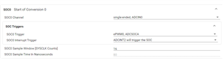
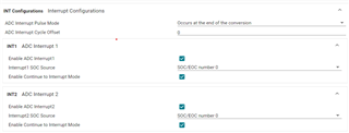
    1. ADCs in the example are triggered by their own INT. is this same in your project? if not what is the source for trigger and are they synchronous
    2. but when i set sampling rate to 4MSPS ( by changing the adc clk prescaler)
      what is the prescaler configuration change you have tried ? and what is the s/h value along with this? 

    Thanks and regards,

    Madhava

  • Hi Madhava,

    1. Yes ADCs are triggered by their own INT.

         Approch is mentioned below-

         a) First ADC conversion is done using ePWM0, ADCSOCA. INT1, INT2 is generated at the end of conversion.

         b) ADC0_INT1 is linked to INT_XBAR_0 for generating interrupt.

         c) When interrupt is received after first converion, I am disabling the ePWM trigger and ADC0_INT1.

         d) From this point onwards INT2 is used to start the interrupt for conversion.


    2. I have assigned  S/H window to 16 (sysclk cycle) which is 80ns for all cases. 

        When i am doing ADCCLK = (input clock) / 4.5 ( sampling rate = 3.2 MSPS approx) it works fine for 2 ADC channel.

        When i make Adc Prescaler 3 or below ( sampling rate >= 4MSPS approx) then there is some phase difference while sampling 2 signal
        of higher frequency.

        Below is formula from which i am calculating sampling rate.


      The main problem comes when i am sampling 4 ADCs simultaneously, Then there is phase difference even for sampling rate of 3.2MSPS.
       
      I have already shared the details of DMA PaRAM configuration in previous response.

      Thanks.


  • Hi Madava,

    Waiting for your reply

  • Hi Tej, 

    Apologies for delayed response, I was out of office. 

      The main problem comes when i am sampling 4 ADCs simultaneously, Then there is phase difference even for sampling rate of 3.2MSPS.

    So, at a sampling rate of 3.2 MSPS as well, you are facing the phase differences? Could you share your observation at 3.2 MSPS, 4 ADC simultaneous? 

    Thanks and regards,

    Madhava


  • Hi Madhava,

    Yes even at sampling rate of 3.2 MSPS i am facing the phase difference issue.


    This is the observation i am getting for 4 ADC simultaneous sampling.

    The sequence in which i am calling App_dmaConfigure function is given below -

    App_dmaConfigure(gAdc1DataBuffer, RESULTS_BUFFER_SIZE, gEdmaHandle[0],
    ADC1_EDMA_CHANNEL, CONFIG_ADC1_RESULT_BASE_ADDR, &tccAlloc0, EDMA_TEST_EVT_QUEUE_NO_0);

    App_dmaConfigure(gAdc2DataBuffer, RESULTS_BUFFER_SIZE, gEdmaHandle[0],
    ADC2_EDMA_CHANNEL, CONFIG_ADC2_RESULT_BASE_ADDR, &tccAlloc1, EDMA_TEST_EVT_QUEUE_NO_1);

    App_dmaConfigure(gAdc3DataBuffer, RESULTS_BUFFER_SIZE, gEdmaHandle[0],
    ADC3_EDMA_CHANNEL, CONFIG_ADC3_RESULT_BASE_ADDR, &tccAlloc2, EDMA_TEST_EVT_QUEUE_NO_0);

    App_dmaConfigure(gAdc4DataBuffer, RESULTS_BUFFER_SIZE, gEdmaHandle[0],
    ADC4_EDMA_CHANNEL, CONFIG_ADC4_RESULT_BASE_ADDR, &tccAlloc3, EDMA_TEST_EVT_QUEUE_NO_1);


    uint16_t App_dmaConfigure(
            const uint16_t *table, uint16_t table_size,
            EDMA_Handle dma_handle, uint32_t dma_ch,
            uint32_t adc_base, uint32_t *tccAlloc, uint32_t event_queue_number)
    {
    
        uint32_t            baseAddr, regionId;
        EDMACCPaRAMEntry    empty_edmaParam, edmaParam;
        uint32_t            empty_dmaCh, dmaCh, empty_tcc, tcc, empty_param, param;
        // EDMACCPaRAMEntry    empty_edmaParam;
        // uint32_t            empty_dmaCh, empty_tcc, empty_param;
        int32_t             testStatus = SystemP_SUCCESS;
    
        uint32_t chainOptions = (EDMA_OPT_TCCHEN_MASK |
                                 EDMA_OPT_ITCCHEN_MASK);
    
        baseAddr = EDMA_getBaseAddr(gEdmaHandle[0]);
        DebugP_assert(baseAddr != 0);
    
        regionId = EDMA_getRegionId(gEdmaHandle[0]);
        DebugP_assert(regionId < SOC_EDMA_NUM_REGIONS);
    
    
        empty_dmaCh = dma_ch;
        testStatus = EDMA_allocDmaChannel(gEdmaHandle[0], &empty_dmaCh);
        DebugP_assert(testStatus == SystemP_SUCCESS);
    
        empty_tcc = EDMA_RESOURCE_ALLOC_ANY;
        testStatus = EDMA_allocTcc(gEdmaHandle[0], &empty_tcc);
        DebugP_assert(testStatus == SystemP_SUCCESS);
    
        empty_param = EDMA_RESOURCE_ALLOC_ANY;
        testStatus = EDMA_allocParam(gEdmaHandle[0], &empty_param);
        DebugP_assert(testStatus == SystemP_SUCCESS);
    
        dmaCh = EDMA_RESOURCE_ALLOC_ANY;
        testStatus = EDMA_allocDmaChannel(gEdmaHandle[0], &dmaCh);
        DebugP_assert(testStatus == SystemP_SUCCESS);
        printf("allocated dma channel %d \n",dmaCh);
        tcc = EDMA_RESOURCE_ALLOC_ANY;
        testStatus = EDMA_allocTcc(gEdmaHandle[0], &tcc);
        DebugP_assert(testStatus == SystemP_SUCCESS);
        /* Passing back the Channel parameter to register the interrupt ISR*/
        *tccAlloc = tcc;
        printf("counter assigned %d \n",counter++);
        param = EDMA_RESOURCE_ALLOC_ANY;
        testStatus = EDMA_allocParam(gEdmaHandle[0], &param);
        DebugP_assert(testStatus == SystemP_SUCCESS);
    
        /* Request channel */
        EDMA_configureChannelRegion(baseAddr, regionId, EDMA_CHANNEL_TYPE_DMA,
             empty_dmaCh, empty_tcc, empty_param, event_queue_number);
    
        /* Program Param Set */
        EDMA_ccPaRAMEntry_init(&empty_edmaParam);
        empty_edmaParam.srcAddr       = (uint32_t) SOC_virtToPhy((void *)(adc_base+CSL_ADC_RESULT_ADCRESULT0));
        empty_edmaParam.destAddr      = (uint32_t) SOC_virtToPhy((void *)gUnusedBuffer);
        empty_edmaParam.aCnt          = (uint16_t) 2;
        empty_edmaParam.bCnt          = (uint16_t) table_size;
        empty_edmaParam.cCnt          = (uint16_t) 1;
        empty_edmaParam.bCntReload    = 0;
        empty_edmaParam.srcBIdx       = (int16_t) EDMA_PARAM_BIDX(0);
        empty_edmaParam.destBIdx      = (int16_t) EDMA_PARAM_BIDX(2);
        empty_edmaParam.srcCIdx       = (int16_t) 0;
        empty_edmaParam.destCIdx      = (int16_t) 0;
        empty_edmaParam.linkAddr      = 0xFFFFU;
        empty_edmaParam.srcBIdxExt    = (int8_t) EDMA_PARAM_BIDX_EXT(0);
        empty_edmaParam.destBIdxExt   = (int8_t) EDMA_PARAM_BIDX_EXT(2);
        empty_edmaParam.opt           = (EDMA_OPT_TCINTEN_MASK | EDMA_OPT_ITCINTEN_MASK |
                                  ((((uint32_t)empty_tcc) << EDMA_OPT_TCC_SHIFT) & EDMA_OPT_TCC_MASK));
    
    
        EDMA_setPaRAM(baseAddr, empty_param, &empty_edmaParam);
    
        EDMA_configureChannelRegion(baseAddr, regionId, EDMA_CHANNEL_TYPE_DMA, dmaCh, tcc, param, event_queue_number);
    
        /* Program Param Set */
        EDMA_ccPaRAMEntry_init(&edmaParam);
        edmaParam.srcAddr       = (uint32_t) SOC_virtToPhy((void *)(adc_base+CSL_ADC_RESULT_ADCRESULT0));
        edmaParam.destAddr      = (uint32_t) SOC_virtToPhy((void *)table);
        edmaParam.aCnt          = (uint16_t) 2;
        edmaParam.bCnt          = (uint16_t) table_size;
        edmaParam.cCnt          = (uint16_t) 1;
        edmaParam.bCntReload    = 0;
        edmaParam.srcBIdx       = (int16_t) EDMA_PARAM_BIDX(0);
        edmaParam.destBIdx      = (int16_t) EDMA_PARAM_BIDX(2);
        edmaParam.srcCIdx       = (int16_t) 0;
        edmaParam.destCIdx      = (int16_t) 0;
        edmaParam.linkAddr      = 0xFFFFU;
        edmaParam.srcBIdxExt    = (int8_t) EDMA_PARAM_BIDX_EXT(0);
        edmaParam.destBIdxExt   = (int8_t) EDMA_PARAM_BIDX_EXT(2);
        edmaParam.opt           = (EDMA_OPT_TCINTEN_MASK |
                                  ((((uint32_t)tcc) << EDMA_OPT_TCC_SHIFT) & EDMA_OPT_TCC_MASK));
    
        /* Enabling the Interrupt for Transfer complete of all the data */
        EDMA_setPaRAM(baseAddr, param, &edmaParam);
    
    
        EDMA_chainChannel(baseAddr, empty_param, dmaCh, chainOptions);
    
        EDMA_enableTransferRegion(baseAddr, regionId, empty_dmaCh,
                                  EDMA_TRIG_MODE_EVENT);
        return testStatus;
    }
    
    
    void App_dmach0ISR(Edma_IntrHandle intrHandle, void *args)
    {
        SemaphoreP_Object *semObjPtr = (SemaphoreP_Object *)args;
        DebugP_assert(semObjPtr != NULL);
        printf("inside the interrupt \n");
       
        ADC_setInterruptSOCTrigger(gAdc1baseAddr, ADC_SOC_NUMBER0,
                                   ADC_INT_SOC_TRIGGER_NONE);
        ADC_setInterruptSOCTrigger(gAdc2baseAddr, ADC_SOC_NUMBER0,
                                   ADC_INT_SOC_TRIGGER_NONE);
        ADC_setInterruptSOCTrigger(gAdc3baseAddr, ADC_SOC_NUMBER0,
                                   ADC_INT_SOC_TRIGGER_NONE);
    
        /* Post the semaphore to signal end of DMA transfer */
        SemaphoreP_post(semObjPtr);
    }


  • Hi Tej,

    I was expecting at least few were in sync assuming they all are sampling same waveform. Few follow up questions,

    1. this phase differences amongst ADCs, are they always constant in different runs or random? I am trying to understand if the ADC's Sampling is async-ed.
    2. Are the ADC's starting from reset for each run? - trying to understand if the configurations from previous runs are overlapping.

    Thanks,

    Madhava 

  • Hii Madhava,

    1- No, Phase difference amongs ADC's are not constant in different runs.

    2- No, ADC's are not starting from reset from each run.

        When I start ADC conversion from reset for each run, it get stuck and DMA tranfer callback funtion is not executed for first few run, after that it runs.

        I think this might be making them asynchronized.

    How to resolve that issue??

  • Hi Tej,

    Please make sure that the ADCs are sampling from reset as that makes them synchronous. The initial trigger from the EPWM is making the ADCs start synchronously. but when the ADCs are not sampling from reset, then the current on-going INT are already triggering SOCs and DMA for transfers is my suspicion.

    thanks,

    Madhava 

  • Hii Madhava,

    When i am sampling ADCs from the reset this is the graph i am getting ( Graph is for the 100KHz signal getting sampled at 4MSPS).


    problem which i am facing is-

    1) For 100KHz signal sampling at 4MSPS we should get 40 samples per cycle but i am getting only 20 samples.


    There is one doubt from my side-

    We will receive the interrupt for end of conversion simultaneously from 4 ADC channel, then how can 2 transfer controllers make then synchronized for simultaneous sampling?


    How to solve this problem??

    Thanks.

  • Hi Tej,

    Could you please clarify if the problem related to 4 ADCs with Synced transfer closed? - the original question in the thread. 

    For 100KHz signal sampling at 4MSPS we should get 40 samples per cycle but i am getting only 20 samples.

    I agree that there should be 40 samples. I see your B_cnt is table_size, what is the value you are passing here? I see your dest_B_indx  and a_cnt are 2, is your destination buffer of size 16 bit? Is your graph picking16 bit values as well? you might be taking a dump of the values from memory browser and plotting this graph, could you share your mem-dump here? 

    There is one doubt from my side-

    We will receive the interrupt for end of conversion simultaneously from 4 ADC channel, then how can 2 transfer controllers make then synchronized for simultaneous sampling?

    The ADC sample+conversion time is around 250ns, and the DMA transfers are way faster than this. Also, the ADC controller will transfer the results from the conversion to the Result space post conversion. hence the DMA has a lot of time to close the current transfer before the new result latches.

    Thanks and regards,

    Madhava 

  • Hi Madhava,
      

    1. Yes the destination buffer size is 16 bit.


    2. This is the details of memory dump file.

    Dump Summary
    ------------
    Dump File:	ccstudio.DMP : C:\Users\vishn\AppData\Local\Temp\ccstudio.DMP
    Last Write Time:	01-07-2024 15:36:06
    Process Name:	C:\ti\ccs1260\ccs\eclipse\ccstudio.exe 
    Process Architecture:	x64
    Exception Code:	not found
    Exception Information:	
    Heap Information:	Present
    
    System Information
    ------------------
    OS Version:	10.0.22631
    CLR Version(s):	
    
    Modules
    -------
    Module Name	Module Path	Module Version
    -----------	-----------	--------------
    ccstudio.exe	C:\ti\ccs1260\ccs\eclipse\ccstudio.exe	0.0.0.0
    ntdll.dll	C:\Windows\System32\ntdll.dll	10.0.22621.3733
    kernel32.dll	C:\Windows\System32\kernel32.dll	10.0.22621.3672
    KERNELBASE.dll	C:\Windows\System32\KERNELBASE.dll	10.0.22621.3733
    user32.dll	C:\Windows\System32\user32.dll	10.0.22621.3672
    win32u.dll	C:\Windows\System32\win32u.dll	10.0.22621.3733
    gdi32.dll	C:\Windows\System32\gdi32.dll	10.0.22621.3672
    gdi32full.dll	C:\Windows\System32\gdi32full.dll	10.0.22621.3672
    msvcp_win.dll	C:\Windows\System32\msvcp_win.dll	10.0.22621.3374
    ucrtbase.dll	C:\Windows\System32\ucrtbase.dll	10.0.22621.3593
    comctl32.dll	C:\Windows\WinSxS\amd64_microsoft.windows.common-controls_6595b64144ccf1df_6.0.22621.3672_none_2713b9d173822955\comctl32.dll	6.10.22621.3672
    msvcrt.dll	C:\Windows\System32\msvcrt.dll	7.0.22621.2506
    imm32.dll	C:\Windows\System32\imm32.dll	10.0.22621.3374
    eclipse_11602.dll	C:\ti\ccs1260\ccs\eclipse\plugins\org.eclipse.equinox.launcher.win32.win32.x86_64_1.2.400.v20211117-0650\eclipse_11602.dll	0.0.0.0
    advapi32.dll	C:\Windows\System32\advapi32.dll	10.0.22621.3733
    sechost.dll	C:\Windows\System32\sechost.dll	10.0.22621.3733
    bcrypt.dll	C:\Windows\System32\bcrypt.dll	10.0.22621.2506
    rpcrt4.dll	C:\Windows\System32\rpcrt4.dll	10.0.22621.3672
    ole32.dll	C:\Windows\System32\ole32.dll	10.0.22621.3672
    combase.dll	C:\Windows\System32\combase.dll	10.0.22621.3672
    version.dll	C:\Windows\System32\version.dll	10.0.22621.1
    uxtheme.dll	C:\Windows\System32\uxtheme.dll	10.0.22621.3672
    msctf.dll	C:\Windows\System32\msctf.dll	10.0.22621.3672
    kernel.appcore.dll	C:\Windows\System32\kernel.appcore.dll	10.0.22621.2715
    bcryptPrimitives.dll	C:\Windows\System32\bcryptPrimitives.dll	10.0.22621.3672
    clbcatq.dll	C:\Windows\System32\clbcatq.dll	2001.12.10941.16384
    textinputframework.dll	C:\Windows\System32\textinputframework.dll	10.0.22621.3672
    oleaut32.dll	C:\Windows\System32\oleaut32.dll	10.0.22621.3672
    CoreMessaging.dll	C:\Windows\System32\CoreMessaging.dll	10.0.22621.3672
    CoreUIComponents.dll	C:\Windows\System32\CoreUIComponents.dll	10.0.22621.3672
    WinTypes.dll	C:\Windows\System32\WinTypes.dll	10.0.22621.3672
    CRYPTBASE.DLL	C:\Windows\System32\CRYPTBASE.DLL	10.0.22621.1
    jvm.dll	C:\ti\ccs1260\ccs\eclipse\jre\bin\server\jvm.dll	11.0.13.0
    psapi.dll	C:\Windows\System32\psapi.dll	10.0.22621.1
    winmm.dll	C:\Windows\System32\winmm.dll	10.0.22621.3672
    wsock32.dll	C:\Windows\System32\wsock32.dll	10.0.22621.1
    VCRUNTIME140.dll	C:\Windows\System32\VCRUNTIME140.dll	14.38.33135.0
    ws2_32.dll	C:\Windows\System32\ws2_32.dll	10.0.22621.1
    verify.dll	C:\ti\ccs1260\ccs\eclipse\jre\bin\verify.dll	11.0.13.0
    dbghelp.dll	C:\Windows\System32\dbghelp.dll	10.0.22621.3593
    dbgcore.dll	C:\Windows\System32\dbgcore.dll	10.0.22621.1
    java.dll	C:\ti\ccs1260\ccs\eclipse\jre\bin\java.dll	11.0.13.0
    jimage.dll	C:\ti\ccs1260\ccs\eclipse\jre\bin\jimage.dll	11.0.13.0
    zip.dll	C:\ti\ccs1260\ccs\eclipse\jre\bin\zip.dll	11.0.13.0
    shell32.dll	C:\Windows\System32\shell32.dll	10.0.22621.3733
    windows.storage.dll	C:\Windows\System32\windows.storage.dll	10.0.22621.3733
    SHCore.dll	C:\Windows\System32\SHCore.dll	10.0.22621.3733
    shlwapi.dll	C:\Windows\System32\shlwapi.dll	10.0.22621.3672
    profapi.dll	C:\Windows\System32\profapi.dll	10.0.22621.3527
    net.dll	C:\ti\ccs1260\ccs\eclipse\jre\bin\net.dll	11.0.13.0
    winhttp.dll	C:\Windows\System32\winhttp.dll	10.0.22621.3672
    mswsock.dll	C:\Windows\System32\mswsock.dll	10.0.22621.2506
    nio.dll	C:\ti\ccs1260\ccs\eclipse\jre\bin\nio.dll	11.0.13.0
    cryptsp.dll	C:\Windows\System32\cryptsp.dll	10.0.22621.3672
    rsaenh.dll	C:\Windows\System32\rsaenh.dll	10.0.22621.1
    userenv.dll	C:\Windows\System32\userenv.dll	10.0.22621.3527
    IPHLPAPI.DLL	C:\Windows\System32\IPHLPAPI.DLL	10.0.22621.1
    nsi.dll	C:\Windows\System32\nsi.dll	10.0.22621.1
    dhcpcsvc6.DLL	C:\Windows\System32\dhcpcsvc6.DLL	10.0.22621.2506
    dhcpcsvc.dll	C:\Windows\System32\dhcpcsvc.dll	10.0.22621.2506
    dnsapi.dll	C:\Windows\System32\dnsapi.dll	10.0.22621.3733
    swt-win32-4950r5.dll	C:\ti\ccs1260\ccs\eclipse\configuration\org.eclipse.osgi\488\0\.cp\swt-win32-4950r5.dll	4.950.5.0
    comdlg32.dll	C:\Windows\System32\comdlg32.dll	10.0.22621.3672
    winspool.drv	C:\Windows\System32\winspool.drv	10.0.22621.3672
    oleacc.dll	C:\Windows\System32\oleacc.dll	7.2.22621.1
    usp10.dll	C:\Windows\System32\usp10.dll	10.0.22621.1
    wininet.dll	C:\Windows\System32\wininet.dll	11.0.22621.2506
    propsys.dll	C:\Windows\System32\propsys.dll	7.0.22621.3672
    msimg32.dll	C:\Windows\System32\msimg32.dll	10.0.22621.2506
    urlmon.dll	C:\Windows\System32\urlmon.dll	11.0.22621.3733
    dwmapi.dll	C:\Windows\System32\dwmapi.dll	10.0.22621.3672
    iertutil.dll	C:\Windows\System32\iertutil.dll	11.0.22621.3672
    srvcli.dll	C:\Windows\System32\srvcli.dll	10.0.22621.3374
    netutils.dll	C:\Windows\System32\netutils.dll	10.0.22621.2506
    swt-gdip-win32-4950r5.dll	C:\ti\ccs1260\ccs\eclipse\configuration\org.eclipse.osgi\488\0\.cp\swt-gdip-win32-4950r5.dll	4.950.5.0
    GdiPlus.dll	C:\Windows\WinSxS\amd64_microsoft.windows.gdiplus_6595b64144ccf1df_1.1.22621.3672_none_57feacb6ce14a323\GdiPlus.dll	10.0.22621.3672
    WindowsCodecs.dll	C:\Windows\System32\WindowsCodecs.dll	10.0.22621.3672
    TextShaping.dll	C:\Windows\System32\TextShaping.dll	10.0.22621.3672
    mlang.dll	C:\Windows\System32\mlang.dll	10.0.22621.1
    localfile_1_0_0.dll	C:\ti\ccs1260\ccs\eclipse\configuration\org.eclipse.osgi\285\0\.cp\os\win32\x86_64\localfile_1_0_0.dll	0.0.0.0
    win32refresh.dll	C:\ti\ccs1260\ccs\eclipse\configuration\org.eclipse.osgi\290\0\.cp\os\win32\x86_64\win32refresh.dll	0.0.0.0
    dataexchange.dll	C:\Windows\System32\dataexchange.dll	10.0.22621.3672
    twinapi.appcore.dll	C:\Windows\System32\twinapi.appcore.dll	10.0.22621.3672
    LibraryLoader.dll	C:\ti\ccs1260\ccs\ccs_base\DebugServer\bin\LibraryLoader.dll	12.6.0.3269
    msvcp140.dll	C:\Windows\System32\msvcp140.dll	14.38.33135.0
    VCRUNTIME140_1.dll	C:\Windows\System32\VCRUNTIME140_1.dll	14.38.33135.0
    ti_logger.dll	C:\ti\ccs1260\ccs\ccs_base\common\bin\ti_logger.dll	12.6.0.3269
    CCReg.dll	C:\ti\ccs1260\ccs\ccs_base\common\bin\CCReg.dll	12.6.0.3269
    fsutil.dll	C:\ti\ccs1260\ccs\ccs_base\common\bin\fsutil.dll	12.6.0.3269
    libusb-1.0.dll	C:\ti\ccs1260\ccs\ccs_base\common\bin\libusb-1.0.dll	1.0.19.10903
    MiniDump.dll	C:\ti\ccs1260\ccs\ccs_base\common\bin\MiniDump.dll	12.6.0.3269
    setup_parser.dll	C:\ti\ccs1260\ccs\ccs_base\common\bin\setup_parser.dll	12.6.0.3269
    xerces-c_2_8.dll	C:\ti\ccs1260\ccs\ccs_base\common\bin\xerces-c_2_8.dll	2.8.0.0
    ti_targetdb_parser.dll	C:\ti\ccs1260\ccs\ccs_base\common\bin\ti_targetdb_parser.dll	5.0.2.0
    ti_xpcom.dll	C:\ti\ccs1260\ccs\ccs_base\DebugServer\bin\ti_xpcom.dll	12.6.0.3269
    DirectoryService.dll	C:\ti\ccs1260\ccs\ccs_base\DebugServer\bin\DirectoryService.dll	12.6.0.3269
    XPCOMUtility.dll	C:\ti\ccs1260\ccs\ccs_base\DebugServer\bin\XPCOMUtility.dll	12.6.0.3269
    DWrite.dll	C:\Windows\System32\DWrite.dll	10.0.22621.3672
    toolkit64.dll	C:\ti\ccs1260\ccs\eclipse\configuration\.jxbrowser.bin\7.29\toolkit64.dll	0.0.0.0
    ipc64.dll	C:\ti\ccs1260\ccs\eclipse\configuration\.jxbrowser.bin\7.29\ipc64.dll	0.0.0.0
    XPCOMTILogger.dll	C:\ti\ccs1260\ccs\ccs_base\DebugServer\bin\XPCOMTILogger.dll	12.6.0.3269
    explorerframe.dll	C:\Windows\System32\explorerframe.dll	10.0.22621.3672
    jWinHttp-1.0.0.dll	C:\ti\ccs1260\ccs\eclipse\configuration\org.eclipse.osgi\288\0\.cp\jWinHttp-1.0.0.dll	0.0.0.0
    rasadhlp.dll	C:\Windows\System32\rasadhlp.dll	10.0.22621.1
    proxy_vole5503326919132165432.dll	C:\Users\vishn\AppData\Local\Temp\proxy_vole5503326919132165432.dll	0.0.0.0
    edputil.dll	C:\Windows\System32\edputil.dll	10.0.22621.3527
    cToolsIF.dll	C:\ti\ccs1260\ccs\ccs_base\emulation\analysis\bin\cToolsIF.dll	2.1.0.0
    ctools.dll	C:\ti\ccs1260\ccs\ccs_base\emulation\analysis\bin\ctools.dll	2.3.0.0
    TraceFactory.dll	C:\ti\ccs1260\ccs\ccs_base\emulation\analysis\bin\TraceFactory.dll	0.0.0.0
    sqlite3.dll	C:\ti\ccs1260\ccs\ccs_base\emulation\analysis\bin\sqlite3.dll	0.0.0.0
    CloudTrace.dll	C:\ti\ccs1260\ccs\ccs_base\emulation\analysis\bin\CloudTrace.dll	0.0.0.0
    AETPropertyHelper.dll	C:\ti\ccs1260\ccs\ccs_base\emulation\analysis\bin\AETPropertyHelper.dll	1.2.0.0
    ti_aett_session.dll	C:\ti\ccs1260\ccs\ccs_base\emulation\analysis\bin\ti_aett_session.dll	0.0.0.0
    sunmscapi.dll	C:\ti\ccs1260\ccs\eclipse\jre\bin\sunmscapi.dll	11.0.13.0
    crypt32.dll	C:\Windows\System32\crypt32.dll	10.0.22621.3672
    ncrypt.dll	C:\Windows\System32\ncrypt.dll	10.0.22621.3672
    ntasn1.dll	C:\Windows\System32\ntasn1.dll	10.0.22621.1
    sunec.dll	C:\ti\ccs1260\ccs\eclipse\jre\bin\sunec.dll	11.0.13.0
    management.dll	C:\ti\ccs1260\ccs\eclipse\jre\bin\management.dll	11.0.13.0
    management_ext.dll	C:\ti\ccs1260\ccs\eclipse\jre\bin\management_ext.dll	11.0.13.0
    DebugServer.dll	C:\ti\ccs1260\ccs\ccs_base\DebugServer\bin\DebugServer.dll	12.6.0.3269
    tiofr11.dll	C:\ti\ccs1260\ccs\ccs_base\DebugServer\bin\tiofr11.dll	12.6.0.3269
    NapiNSP.dll	C:\Windows\System32\NapiNSP.dll	10.0.22621.1
    pnrpnsp.dll	C:\Windows\System32\pnrpnsp.dll	10.0.22621.1
    winrnr.dll	C:\Windows\System32\winrnr.dll	10.0.22621.1
    nlansp_c.dll	C:\Windows\System32\nlansp_c.dll	10.0.22621.3672
    wshbth.dll	C:\Windows\System32\wshbth.dll	10.0.22621.3374
    FWPUCLNT.DLL	C:\Windows\System32\FWPUCLNT.DLL	10.0.22621.3235
    ninput.dll	C:\Windows\System32\ninput.dll	10.0.22621.3672
    DebugProperties.dll	C:\ti\ccs1260\ccs\ccs_base\DebugServer\bin\DebugProperties.dll	12.6.0.3269
    spawner.dll	C:\ti\ccs1260\ccs\eclipse\plugins\org.eclipse.cdt.core.win32.x86_64_6.0.500.202203091838\os\win32\x86_64\spawner.dll	0.0.0.0
    ntmarta.dll	C:\Windows\System32\ntmarta.dll	10.0.22621.1
    GTIRemoteProxy.dll	C:\ti\ccs1260\ccs\ccs_base\DebugServer\bin\GTIRemoteProxy.dll	12.6.0.3269
    jtagdata.dll	C:\ti\ccs1260\ccs\ccs_base\common\uscif\jtagdata.dll	35.35.0.0
    cfgmgr32.dll	C:\Windows\System32\cfgmgr32.dll	10.0.22621.2506
    setupapi.dll	C:\Windows\System32\setupapi.dll	10.0.22621.2506
    winusb.dll	C:\Windows\System32\winusb.dll	10.0.22621.1
    hid.dll	C:\Windows\System32\hid.dll	10.0.22621.1
    devobj.dll	C:\Windows\System32\devobj.dll	10.0.22621.2506
    wintrust.dll	C:\Windows\System32\wintrust.dll	10.0.22621.3737
    msasn1.dll	C:\Windows\System32\msasn1.dll	10.0.22621.2506
    ti_aett_logger.dll	C:\ti\ccs1260\ccs\ccs_base\emulation\analysis\bin\ti_aett_logger.dll	0.0.0.0
    ti_aett_setup_manager.DLL	C:\ti\ccs1260\ccs\ccs_base\emulation\analysis\bin\ti_aett_setup_manager.DLL	0.0.0.0
    ICETargetAdapter.DLL	C:\ti\ccs1260\ccs\ccs_base\emulation\analysis\bin\ICETargetAdapter.DLL	1.3.0.0
    IceCD.dll	C:\ti\ccs1260\ccs\ccs_base\emulation\analysis\bin\IceCD.dll	1.3.0.0
    ti_aett_database.dll	C:\ti\ccs1260\ccs\ccs_base\emulation\analysis\bin\ti_aett_database.dll	0.0.0.0
    lldbSM.dll	C:\ti\ccs1260\ccs\ccs_base\DebugServer\bin\lldbSM.dll	16.0.1310.0
    System_xmtr.DLL	C:\ti\ccs1260\ccs\ccs_base\emulation\analysis\bin\System_xmtr.DLL	0.0.0.0
    proxy_vole8770055297768816587.dll	C:\Users\vishn\AppData\Local\Temp\proxy_vole8770055297768816587.dll	0.0.0.0
    awt.dll	C:\ti\ccs1260\ccs\eclipse\jre\bin\awt.dll	11.0.13.0
    apphelp.dll	C:\Windows\System32\apphelp.dll	10.0.22621.3672
    WebView2Loader.dll	C:\ti\ccs1260\ccs\eclipse\configuration\org.eclipse.osgi\488\0\.cp\WebView2Loader.dll	1.0.721.0
    EmbeddedBrowserWebView.dll	C:\Program Files (x86)\Microsoft\EdgeWebView\Application\126.0.2592.68\EBWebView\x64\EmbeddedBrowserWebView.dll	126.0.2592.68
    sspicli.dll	C:\Windows\System32\sspicli.dll	10.0.22621.3672
    Windows.System.Launcher.dll	C:\Windows\System32\Windows.System.Launcher.dll	10.0.22621.3672
    msvcp110_win.dll	C:\Windows\System32\msvcp110_win.dll	10.0.22621.1
    windows.staterepositorycore.dll	C:\Windows\System32\windows.staterepositorycore.dll	10.0.22621.3672
    AETProperties.DLL	C:\ti\ccs1260\ccs\ccs_base\emulation\analysis\bin\AETProperties.DLL	0.0.0.0
    tixds510debugssm.dvr	C:\ti\ccs1260\ccs\ccs_base\emulation\drivers\tixds510debugssm.dvr	1.0.0.0
    xdsfast3.dll	C:\ti\ccs1260\ccs\ccs_base\common\uscif\xdsfast3.dll	35.35.0.0
    prsc.dll	C:\ti\ccs1260\ccs\ccs_base\emulation\drivers\prsc.dll	5.1.2.0
    tixds510cs_dap.dvr	C:\ti\ccs1260\ccs\ccs_base\emulation\drivers\tixds510cs_dap.dvr	5.0.1.0
    cmapi.dll	C:\ti\ccs1260\ccs\ccs_base\emulation\drivers\cmapi.dll	1.1.0.0
    jscxds110.dll	C:\ti\ccs1260\ccs\ccs_base\common\uscif\jscxds110.dll	35.35.0.0
    tixds510cortexR.dvr	C:\ti\ccs1260\ccs\ccs_base\emulation\drivers\tixds510cortexR.dvr	11.0.2.0
    tixds510cortexM.dvr	C:\ti\ccs1260\ccs\ccs_base\emulation\drivers\tixds510cortexM.dvr	11.2.2.0
    tixds510pru.dvr	C:\ti\ccs1260\ccs\ccs_base\emulation\drivers\tixds510pru.dvr	2.0.2.0
    tixds510csstm.dvr	C:\ti\ccs1260\ccs\ccs_base\emulation\drivers\tixds510csstm.dvr	4.0.1.0
    tixds510etbcs.dvr	C:\ti\ccs1260\ccs\ccs_base\emulation\drivers\tixds510etbcs.dvr	4.1.1.0
    tpi_icepick.dll	C:\ti\ccs1260\ccs\ccs_base\emulation\tpi\tpi_icepick.dll	4.0.1.0
    xdsboard.dll	C:\ti\ccs1260\ccs\ccs_base\common\uscif\xdsboard.dll	35.35.0.0
    tpi_cs_dap.dll	C:\ti\ccs1260\ccs\ccs_base\emulation\tpi\tpi_cs_dap.dll	5.0.1.0
    tpiarm_x.dll	C:\ti\ccs1260\ccs\ccs_base\emulation\tpi\tpiarm_x.dll	34.0.0.0
    tpi_ihwa.dll	C:\ti\ccs1260\ccs\ccs_base\emulation\tpi\tpi_ihwa.dll	5.0.5.0
    tpitrace.dll	C:\ti\ccs1260\ccs\ccs_base\emulation\tpi\tpitrace.dll	4.0.0.0
    tpietb.dll	C:\ti\ccs1260\ccs\ccs_base\emulation\tpi\tpietb.dll	4.0.1.0
    ctoolsndbg.DLL	C:\ti\ccs1260\ccs\ccs_base\emulation\analysis\bin\ctoolsndbg.DLL	2.1.0.0
    TraceOperationServer.DLL	C:\ti\ccs1260\ccs\ccs_base\emulation\analysis\bin\TraceOperationServer.DLL	0.0.0.0
    xdstrove.dll	C:\ti\ccs1260\ccs\ccs_base\common\uscif\xdstrove.dll	35.35.0.0
    xdslocal.dll	C:\ti\ccs1260\ccs\ccs_base\common\uscif\xdslocal.dll	35.35.0.0
    xdsroute.dll	C:\ti\ccs1260\ccs\ccs_base\common\uscif\xdsroute.dll	35.35.0.0
    xdsicicle.dll	C:\ti\ccs1260\ccs\ccs_base\common\uscif\xdsicicle.dll	35.35.0.0
    DeviceIdentifier.DLL	C:\ti\ccs1260\ccs\ccs_base\emulation\analysis\bin\DeviceIdentifier.DLL	0.0.0.0
    ti_aett_radar.DLL	C:\ti\ccs1260\ccs\ccs_base\emulation\analysis\bin\ti_aett_radar.DLL	0.0.0.0
    ct470api.dll	C:\ti\ccs1260\ccs\ccs_base\emulation\analysis\bin\ct470api.dll	0.0.0.0
    FlashSitaraMCU.dll	C:\ti\ccs1260\ccs\ccs_base\DebugServer\bin\FlashSitaraMCU.dll	0.0.0.0


    3. This is image of memory browser.


    Thanks.

  • Hi Tej,

    The Memory Browser image was what I requested. thanks.

    When i am sampling ADCs from the reset this is the graph i am getting ( Graph is for the 100KHz signal getting sampled at 4MSPS).

    This image you have shared, this seems like the samples are not taken at the same time (reason : same sample, different voltage point on the same input). Can you confirm if you had 40 samples per input cycle when you had only 2 DMA channels and 2 ADCs? 

    Also, Could you confirm if you are enabling the ADC SOC trigger from EPWM before or after configuring the DMA channels? 

    Thanks and regards,

    Madhava

  • Hi Madhava,


      1. This is the graph for sampling rate 4MSPS with signal of 100KHz. 
          Number of samples points for each cycle is in range 39-40.
      
      2. I am enabling ADC SOC trigger from EPWM after configuring the DMA channels.

    Thanks.

  • Hi Tej,

    The case 4MSPS with 40 samples on 2 ADCs is good and as expected. Can we check any EDMA err flags in the 4 ADCs case? I am afraid if there are any bottlenecks. 

      2. I am enabling ADC SOC trigger from EPWM after configuring the DMA channe

    Ok. thanks for confirming this. 

    thanks and regards,

    Madhava

  • Hi Madhava,


    This is the value of register during execution of program.

    Can you exactly point out the register whose value you are interested in??
     
    Thanks.

  • Hi Madhava,

    Is there any way to alter the speed of DMA transfer in am-2634?

    Thanks. 

  • Hi Madhava,

    Updates -

        I've conducted further testing with different sampling rate configurations, and I'd like to share the results and seek your insights:

    1. When the sampling rate is set below 2 Msps across all four channels, simultaneous sampling appears to function correctly for all 4 channels.
    2. However, when the sampling rate is increased beyond 2 Msps, the effective sampling rate seems to be capped at 2 Msps, regardless of the configured value. This translates to approximately 20 samples per cycle for a 100 kHz signal, even at higher configured sampling rate.

        Based on these observations, I suspect there might be a limitation on the DMA transfer mechanism that restricts the actual sampling rate when exceeding 2 Msps.

        To facilitate our progress and minimize any potential project delays, I'd greatly appreciate your insights on potential workarounds or alternative approaches to achieve      the desired sampling rates.

    Thanks

  • Hi Tej

    Please give me tomorrow to get this case working in my system and try to bring a solution to you.

    Really apologize for the inconvenience caused!

    Thanks and Regards
    Akshit

  • Hi Akshit Pareek,

    I wanted to check in regarding the case we discussed.
    Have you had a chance to look into it?

    Thanks.

  • Hi Tej,

    Yes I have been working to find a solution.

    Could you share your example.syscfg file with me?

    Thanks
    Akshit

  • Hi Akshit Pareek,

    It's currently outside my working hours, but my system configuration settings looks similar to this

    /**
     * These arguments were used when this file was generated. They will be automatically applied on subsequent loads
     * via the GUI or CLI. Run CLI with '--help' for additional information on how to override these arguments.
     * @cliArgs --device "AM263x_beta" --package "ZCZ" --part "AM263x" --context "r5fss0-0" --product "MCU_PLUS_SDK_AM263x@09.02.00"
     * @versions {"tool":"1.20.0+3587"}
     */
    
    /**
     * Import the modules used in this configuration.
     */
    const adc             = scripting.addModule("/drivers/adc/adc");
    const adc1            = adc.addInstance();
    const adc2            = adc.addInstance();
    const adc3            = adc.addInstance();
    const adc4            = adc.addInstance();
    const edma            = scripting.addModule("/drivers/edma/edma", {}, false);
    const edma1           = edma.addInstance();
    const epwm            = scripting.addModule("/drivers/epwm/epwm", {}, false);
    const epwm1           = epwm.addInstance();
    const debug_log       = scripting.addModule("/kernel/dpl/debug_log");
    const mpu_armv7       = scripting.addModule("/kernel/dpl/mpu_armv7", {}, false);
    const mpu_armv71      = mpu_armv7.addInstance();
    const mpu_armv72      = mpu_armv7.addInstance();
    const mpu_armv73      = mpu_armv7.addInstance();
    const mpu_armv74      = mpu_armv7.addInstance();
    const default_linker  = scripting.addModule("/memory_configurator/default_linker", {}, false);
    const default_linker1 = default_linker.addInstance();
    const general         = scripting.addModule("/memory_configurator/general", {}, false);
    const general1        = general.addInstance();
    const region          = scripting.addModule("/memory_configurator/region", {}, false);
    const region1         = region.addInstance();
    const section         = scripting.addModule("/memory_configurator/section", {}, false);
    const section1        = section.addInstance();
    const section2        = section.addInstance();
    const section3        = section.addInstance();
    const section4        = section.addInstance();
    const section5        = section.addInstance();
    const section6        = section.addInstance();
    const section7        = section.addInstance();
    const section8        = section.addInstance();
    const section9        = section.addInstance();
    const section10       = section.addInstance();
    const section11       = section.addInstance();
    const section12       = section.addInstance();
    const int_xbar        = scripting.addModule("/xbar/int_xbar/int_xbar", {}, false);
    const int_xbar1       = int_xbar.addInstance();
    
    /**
     * Write custom configuration values to the imported modules.
     */
    adc.synchronousModeCheck = true;
    
    adc1.$name                          = "CONFIG_ADC1";
    adc1.enableConverter                = true;
    adc1.soc0Trigger                    = "ADC_TRIGGER_EPWM0_SOCA";
    adc1.soc0InterruptTrigger           = "ADC_INT_SOC_TRIGGER_ADCINT2";
    adc1.enableInterrupt2               = true;
    adc1.enableInterrupt2ContinuousMode = true;
    adc1.enableInterrupt1               = true;
    adc1.adcClockPrescaler              = "ADC_CLK_DIV_3_0";
    adc1.interruptPulseMode             = "ADC_PULSE_END_OF_CONV";
    adc1.socHighPriorityMode            = "ADC_PRI_SOC0_HIPRI";
    adc1.ADC.$assign                    = "ADC0";
    
    adc2.$name                          = "CONFIG_ADC2";
    adc2.enableConverter                = true;
    adc2.soc0Trigger                    = "ADC_TRIGGER_EPWM0_SOCA";
    adc2.soc0InterruptTrigger           = "ADC_INT_SOC_TRIGGER_ADCINT2";
    adc2.enableInterrupt2               = true;
    adc2.enableInterrupt2ContinuousMode = true;
    adc2.adcClockPrescaler              = "ADC_CLK_DIV_3_0";
    adc2.interruptPulseMode             = "ADC_PULSE_END_OF_CONV";
    adc2.socHighPriorityMode            = "ADC_PRI_SOC0_HIPRI";
    adc2.ADC.$assign                    = "ADC1";
    
    adc3.$name                          = "CONFIG_ADC3";
    adc3.enableConverter                = true;
    adc3.interruptPulseMode             = "ADC_PULSE_END_OF_CONV";
    adc3.enableInterrupt2               = true;
    adc3.enableInterrupt2ContinuousMode = true;
    adc3.adcClockPrescaler              = "ADC_CLK_DIV_3_0";
    adc3.soc0Trigger                    = "ADC_TRIGGER_EPWM0_SOCA";
    adc3.soc0InterruptTrigger           = "ADC_INT_SOC_TRIGGER_ADCINT2";
    adc3.socHighPriorityMode            = "ADC_PRI_SOC0_HIPRI";
    
    adc4.$name                          = "CONFIG_ADC4";
    adc4.adcClockPrescaler              = "ADC_CLK_DIV_3_0";
    adc4.soc0Trigger                    = "ADC_TRIGGER_EPWM0_SOCA";
    adc4.soc0InterruptTrigger           = "ADC_INT_SOC_TRIGGER_ADCINT2";
    adc4.enableConverter                = true;
    adc4.enableInterrupt2               = true;
    adc4.enableInterrupt2ContinuousMode = true;
    adc4.socHighPriorityMode            = "ADC_PRI_SOC0_HIPRI";
    adc4.interruptPulseMode             = "ADC_PULSE_END_OF_CONV";
    adc4.ADC.$assign                    = "ADC3";
    
    edma1.$name                                         = "CONFIG_EDMA0";
    edma1.edmaRmDmaCh[0].$name                          = "CONFIG_EDMA_RM0";
    edma1.edmaRmQdmaCh[0].$name                         = "CONFIG_EDMA_RM1";
    edma1.edmaRmTcc[0].$name                            = "CONFIG_EDMA_RM2";
    edma1.edmaRmParam[0].$name                          = "CONFIG_EDMA_RM3";
    edma1.edmaChannel.create(4);
    edma1.edmaChannel[0].$name                          = "CONFIG_EDMA_CH0";
    edma1.edmaChannel[0].channelTrigger                 = "ADC0_INT2";
    edma1.edmaChannel[0].xbarConfig.$name               = "CONFIG_DMA_TRIG_XBAR0";
    edma1.edmaChannel[0].xbarConfig.xbarConfig.$name    = "CONFIG_DMA_XBAR0";
    edma1.edmaChannel[1].$name                          = "CONFIG_EDMA_CH1";
    edma1.edmaChannel[1].channelTrigger                 = "ADC1_INT2";
    edma1.edmaChannel[1].xbarConfig.$name               = "CONFIG_DMA_TRIG_XBAR1";
    edma1.edmaChannel[1].xbarConfig.instance            = "DMA_TRIG_XBAR_EDMA_MODULE_2";
    edma1.edmaChannel[1].xbarConfig.xbarConfig.$name    = "CONFIG_DMA_XBAR1";
    edma1.edmaChannel[1].xbarConfig.xbarConfig.instance = "DMA_XBAR_DMA_TRIG_XBAR_2";
    edma1.edmaChannel[2].$name                          = "CONFIG_EDMA_CH2";
    edma1.edmaChannel[2].channelTrigger                 = "ADC2_INT2";
    edma1.edmaChannel[2].xbarConfig.$name               = "CONFIG_DMA_TRIG_XBAR2";
    edma1.edmaChannel[2].xbarConfig.instance            = "DMA_TRIG_XBAR_EDMA_MODULE_4";
    edma1.edmaChannel[2].xbarConfig.xbarConfig.$name    = "CONFIG_DMA_XBAR2";
    edma1.edmaChannel[2].xbarConfig.xbarConfig.instance = "DMA_XBAR_DMA_TRIG_XBAR_4";
    edma1.edmaChannel[3].$name                          = "CONFIG_EDMA_CH3";
    edma1.edmaChannel[3].channelTrigger                 = "ADC3_INT2";
    edma1.edmaChannel[3].xbarConfig.$name               = "CONFIG_DMA_TRIG_XBAR3";
    edma1.edmaChannel[3].xbarConfig.instance            = "DMA_TRIG_XBAR_EDMA_MODULE_6";
    edma1.edmaChannel[3].xbarConfig.xbarConfig.$name    = "CONFIG_DMA_XBAR3";
    edma1.edmaChannel[3].xbarConfig.xbarConfig.instance = "DMA_XBAR_DMA_TRIG_XBAR_6";
    
    epwm1.$name                                                    = "CONFIG_EPWM0";
    epwm1.epwmTimebase_emulationMode                               = "EPWM_EMULATION_FREE_RUN";
    epwm1.epwmTimebase_clockDiv                                    = "EPWM_CLOCK_DIVIDER_4";
    epwm1.epwmTimebase_period                                      = 4000;
    epwm1.epwmCounterCompare_cmpA                                  = 2000;
    epwm1.epwmActionQualifier_EPWM_AQ_OUTPUT_A_ON_TIMEBASE_ZERO    = "EPWM_AQ_OUTPUT_HIGH";
    epwm1.epwmActionQualifier_EPWM_AQ_OUTPUT_A_ON_TIMEBASE_UP_CMPA = "EPWM_AQ_OUTPUT_LOW";
    
    debug_log.enableUartLog            = true;
    debug_log.uartLog.$name            = "CONFIG_UART0";
    debug_log.uartLog.UART.RXD.$assign = "UART0_RXD";
    debug_log.uartLog.UART.TXD.$assign = "UART0_TXD";
    debug_log.uartLog.child.$name      = "drivers_uart_v2_uart_v2_template0";
    
    mpu_armv71.$name             = "CONFIG_MPU_REGION0";
    mpu_armv71.size              = 31;
    mpu_armv71.attributes        = "Device";
    mpu_armv71.accessPermissions = "Supervisor RD+WR, User RD";
    mpu_armv71.allowExecute      = false;
    
    mpu_armv72.$name             = "CONFIG_MPU_REGION1";
    mpu_armv72.size              = 15;
    mpu_armv72.accessPermissions = "Supervisor RD+WR, User RD";
    
    mpu_armv73.$name             = "CONFIG_MPU_REGION2";
    mpu_armv73.baseAddr          = 0x80000;
    mpu_armv73.size              = 15;
    mpu_armv73.accessPermissions = "Supervisor RD+WR, User RD";
    
    mpu_armv74.$name             = "CONFIG_MPU_REGION3";
    mpu_armv74.accessPermissions = "Supervisor RD+WR, User RD";
    mpu_armv74.baseAddr          = 0x70000000;
    mpu_armv74.size              = 21;
    
    default_linker1.$name = "memory_configurator_default_linker0";
    
    general1.$name        = "CONFIG_GENERAL0";
    general1.linker.$name = "TIARMCLANG0";
    
    region1.$name                                = "MEMORY_REGION_CONFIGURATION0";
    region1.memory_region.create(11);
    region1.memory_region[0].type                = "TCMA";
    region1.memory_region[0].$name               = "R5F_VECS";
    region1.memory_region[0].size                = 0x40;
    region1.memory_region[0].auto                = false;
    region1.memory_region[1].type                = "TCMA";
    region1.memory_region[1].$name               = "R5F_TCMA";
    region1.memory_region[1].size                = 0x7FC0;
    region1.memory_region[2].type                = "TCMB";
    region1.memory_region[2].size                = 0x8000;
    region1.memory_region[2].$name               = "R5F_TCMB";
    region1.memory_region[3].$name               = "SBL";
    region1.memory_region[3].auto                = false;
    region1.memory_region[3].size                = 0x40000;
    region1.memory_region[4].$name               = "OCRAM";
    region1.memory_region[4].auto                = false;
    region1.memory_region[4].manualStartAddress  = 0x70040000;
    region1.memory_region[4].size                = 0x40000;
    region1.memory_region[5].type                = "FLASH";
    region1.memory_region[5].auto                = false;
    region1.memory_region[5].size                = 0x80000;
    region1.memory_region[5].$name               = "FLASH";
    region1.memory_region[6].$name               = "USER_SHM_MEM";
    region1.memory_region[6].auto                = false;
    region1.memory_region[6].manualStartAddress  = 0x701D0000;
    region1.memory_region[6].size                = 0x4000;
    region1.memory_region[6].isShared            = true;
    region1.memory_region[6].shared_cores        = ["r5fss0-1","r5fss1-0","r5fss1-1"];
    region1.memory_region[7].$name               = "LOG_SHM_MEM";
    region1.memory_region[7].auto                = false;
    region1.memory_region[7].manualStartAddress  = 0x701D4000;
    region1.memory_region[7].size                = 0x4000;
    region1.memory_region[7].isShared            = true;
    region1.memory_region[7].shared_cores        = ["r5fss0-1","r5fss1-0","r5fss1-1"];
    region1.memory_region[8].type                = "CUSTOM";
    region1.memory_region[8].$name               = "RTOS_NORTOS_IPC_SHM_MEM";
    region1.memory_region[8].auto                = false;
    region1.memory_region[8].manualStartAddress  = 0x72000000;
    region1.memory_region[8].size                = 0x3E80;
    region1.memory_region[8].isShared            = true;
    region1.memory_region[8].shared_cores        = ["r5fss0-1","r5fss1-0","r5fss1-1"];
    region1.memory_region[9].type                = "CUSTOM";
    region1.memory_region[9].$name               = "MAILBOX_HSM";
    region1.memory_region[9].auto                = false;
    region1.memory_region[9].manualStartAddress  = 0x44000000;
    region1.memory_region[9].size                = 0x3CE;
    region1.memory_region[9].isShared            = true;
    region1.memory_region[9].shared_cores        = ["r5fss0-1","r5fss1-0","r5fss1-1"];
    region1.memory_region[10].type               = "CUSTOM";
    region1.memory_region[10].$name              = "MAILBOX_R5F";
    region1.memory_region[10].auto               = false;
    region1.memory_region[10].manualStartAddress = 0x44000400;
    region1.memory_region[10].size               = 0x3CE;
    region1.memory_region[10].isShared           = true;
    region1.memory_region[10].shared_cores       = ["r5fss0-1","r5fss1-0","r5fss1-1"];
    
    section1.load_memory                  = "R5F_VECS";
    section1.group                        = false;
    section1.$name                        = "Vector Table";
    section1.output_section.create(1);
    section1.output_section[0].$name      = ".vectors";
    section1.output_section[0].palignment = true;
    
    section2.load_memory                  = "OCRAM";
    section2.$name                        = "Text Segments";
    section2.output_section.create(5);
    section2.output_section[0].$name      = ".text.hwi";
    section2.output_section[0].palignment = true;
    section2.output_section[1].$name      = ".text.cache";
    section2.output_section[1].palignment = true;
    section2.output_section[2].$name      = ".text.mpu";
    section2.output_section[2].palignment = true;
    section2.output_section[3].$name      = ".text.boot";
    section2.output_section[3].palignment = true;
    section2.output_section[4].$name      = ".text:abort";
    section2.output_section[4].palignment = true;
    
    section3.load_memory                  = "OCRAM";
    section3.$name                        = "Code and Read-Only Data";
    section3.output_section.create(2);
    section3.output_section[0].$name      = ".text";
    section3.output_section[0].palignment = true;
    section3.output_section[1].$name      = ".rodata";
    section3.output_section[1].palignment = true;
    
    section4.load_memory                  = "OCRAM";
    section4.$name                        = "Data Segment";
    section4.output_section.create(1);
    section4.output_section[0].$name      = ".data";
    section4.output_section[0].palignment = true;
    
    section5.load_memory                             = "OCRAM";
    section5.$name                                   = "Memory Segments";
    section5.output_section.create(3);
    section5.output_section[0].$name                 = ".bss";
    section5.output_section[0].output_sections_start = "__BSS_START";
    section5.output_section[0].output_sections_end   = "__BSS_END";
    section5.output_section[0].palignment            = true;
    section5.output_section[1].$name                 = ".sysmem";
    section5.output_section[1].palignment            = true;
    section5.output_section[2].$name                 = ".stack";
    section5.output_section[2].palignment            = true;
    
    section6.load_memory                              = "OCRAM";
    section6.$name                                    = "Stack Segments";
    section6.output_section.create(5);
    section6.output_section[0].$name                  = ".irqstack";
    section6.output_section[0].output_sections_start  = "__IRQ_STACK_START";
    section6.output_section[0].output_sections_end    = "__IRQ_STACK_END";
    section6.output_section[0].input_section.create(1);
    section6.output_section[0].input_section[0].$name = ". = . + __IRQ_STACK_SIZE;";
    section6.output_section[1].$name                  = ".fiqstack";
    section6.output_section[1].output_sections_start  = "__FIQ_STACK_START";
    section6.output_section[1].output_sections_end    = "__FIQ_STACK_END";
    section6.output_section[1].input_section.create(1);
    section6.output_section[1].input_section[0].$name = ". = . + __FIQ_STACK_SIZE;";
    section6.output_section[2].$name                  = ".svcstack";
    section6.output_section[2].output_sections_start  = "__SVC_STACK_START";
    section6.output_section[2].output_sections_end    = "__SVC_STACK_END";
    section6.output_section[2].input_section.create(1);
    section6.output_section[2].input_section[0].$name = ". = . + __SVC_STACK_SIZE;";
    section6.output_section[3].$name                  = ".abortstack";
    section6.output_section[3].output_sections_start  = "__ABORT_STACK_START";
    section6.output_section[3].output_sections_end    = "__ABORT_STACK_END";
    section6.output_section[3].input_section.create(1);
    section6.output_section[3].input_section[0].$name = ". = . + __ABORT_STACK_SIZE;";
    section6.output_section[4].$name                  = ".undefinedstack";
    section6.output_section[4].output_sections_start  = "__UNDEFINED_STACK_START";
    section6.output_section[4].output_sections_end    = "__UNDEFINED_STACK_END";
    section6.output_section[4].input_section.create(1);
    section6.output_section[4].input_section[0].$name = ". = . + __UNDEFINED_STACK_SIZE;";
    
    section7.load_memory                  = "OCRAM";
    section7.$name                        = "Initialization and Exception Handling";
    section7.output_section.create(3);
    section7.output_section[0].$name      = ".ARM.exidx";
    section7.output_section[0].palignment = true;
    section7.output_section[1].$name      = ".init_array";
    section7.output_section[1].palignment = true;
    section7.output_section[2].$name      = ".fini_array";
    section7.output_section[2].palignment = true;
    
    section8.load_memory                 = "USER_SHM_MEM";
    section8.type                        = "NOLOAD";
    section8.$name                       = "User Shared Memory";
    section8.group                       = false;
    section8.output_section.create(1);
    section8.output_section[0].$name     = ".bss.user_shared_mem";
    section8.output_section[0].alignment = 0;
    
    section9.load_memory                 = "LOG_SHM_MEM";
    section9.$name                       = "Log Shared Memory";
    section9.group                       = false;
    section9.type                        = "NOLOAD";
    section9.output_section.create(1);
    section9.output_section[0].$name     = ".bss.log_shared_mem";
    section9.output_section[0].alignment = 0;
    
    section10.load_memory                 = "RTOS_NORTOS_IPC_SHM_MEM";
    section10.type                        = "NOLOAD";
    section10.$name                       = "IPC Shared Memory";
    section10.group                       = false;
    section10.output_section.create(1);
    section10.output_section[0].$name     = ".bss.ipc_vring_mem";
    section10.output_section[0].alignment = 0;
    
    section11.load_memory                 = "MAILBOX_HSM";
    section11.type                        = "NOLOAD";
    section11.$name                       = "SIPC HSM Queue Memory";
    section11.group                       = false;
    section11.output_section.create(1);
    section11.output_section[0].$name     = ".bss.sipc_hsm_queue_mem";
    section11.output_section[0].alignment = 0;
    
    section12.load_memory                 = "MAILBOX_R5F";
    section12.$name                       = "SIPC R5F Queue Memory";
    section12.group                       = false;
    section12.type                        = "NOLOAD";
    section12.output_section.create(1);
    section12.output_section[0].$name     = ".bss.sipc_r5f_queue_mem";
    section12.output_section[0].alignment = 0;
    
    int_xbar1.$name      = "CONFIG_INT_XBAR0";
    int_xbar1.xbarOutput = ["ADC0_INT1"];
    
    /**
     * Pinmux solution for unlocked pins/peripherals. This ensures that minor changes to the automatic solver in a future
     * version of the tool will not impact the pinmux you originally saw.  These lines can be completely deleted in order to
     * re-solve from scratch.
     */
    adc1.ADC.AIN0.$suggestSolution          = "ADC0_AIN0";
    adc1.ADC.AIN1.$suggestSolution          = "ADC0_AIN1";
    adc1.ADC.AIN2.$suggestSolution          = "ADC0_AIN2";
    adc1.ADC.AIN3.$suggestSolution          = "ADC0_AIN3";
    adc1.ADC.AIN4.$suggestSolution          = "ADC0_AIN4";
    adc1.ADC.AIN5.$suggestSolution          = "ADC0_AIN5";
    adc2.ADC.AIN0.$suggestSolution          = "ADC1_AIN0";
    adc2.ADC.AIN1.$suggestSolution          = "ADC1_AIN1";
    adc2.ADC.AIN2.$suggestSolution          = "ADC1_AIN2";
    adc2.ADC.AIN3.$suggestSolution          = "ADC1_AIN3";
    adc2.ADC.AIN4.$suggestSolution          = "ADC1_AIN4";
    adc2.ADC.AIN5.$suggestSolution          = "ADC1_AIN5";
    adc3.ADC.$suggestSolution               = "ADC2";
    adc3.ADC.AIN0.$suggestSolution          = "ADC2_AIN0";
    adc3.ADC.AIN1.$suggestSolution          = "ADC2_AIN1";
    adc3.ADC.AIN2.$suggestSolution          = "ADC2_AIN2";
    adc3.ADC.AIN3.$suggestSolution          = "ADC2_AIN3";
    adc3.ADC.AIN4.$suggestSolution          = "ADC2_AIN4";
    adc3.ADC.AIN5.$suggestSolution          = "ADC2_AIN5";
    adc4.ADC.AIN0.$suggestSolution          = "ADC3_AIN0";
    adc4.ADC.AIN1.$suggestSolution          = "ADC3_AIN1";
    adc4.ADC.AIN2.$suggestSolution          = "ADC3_AIN2";
    adc4.ADC.AIN3.$suggestSolution          = "ADC3_AIN3";
    adc4.ADC.AIN4.$suggestSolution          = "ADC3_AIN4";
    adc4.ADC.AIN5.$suggestSolution          = "ADC3_AIN5";
    epwm1.EPWM.$suggestSolution             = "EPWM0";
    epwm1.EPWM.A.$suggestSolution           = "EPWM0_A";
    epwm1.EPWM.B.$suggestSolution           = "EPWM0_B";
    debug_log.uartLog.UART.$suggestSolution = "UART0";
    
    .

    Thanks.

  • Hi Akshit Pareek,

    I am keen to know if there have been any updates or if you have any further suggestions.

    Thanks.

  • Hi Tej

    Still trying to find a solution, it seems like an issue with transferring all 4 results simultaneously, I'm afraid the DMA channels aren't actually getting free before the next data comes in.

    Please refer to this thread till we debug the issue further: https://e2e.ti.com/support/microcontrollers/arm-based-microcontrollers-group/arm-based-microcontrollers/f/arm-based-microcontrollers-forum/1319076/mcu-plus-sdk-am263x-continuous-sampling-of-multiple-adcs-to-dma-buffers

    Let me know if it helps a bit!

    Apologies and regards
    Akshit

  • Hi Akshit Pareek,

    Thanks for your suggestion,

    I went through the above link, it really helped me to implement the ping-pong buffer. But the problem for simultaneous sampling on 4 channel at 4MSPS still exists.

    Thanks.