This thread has been locked.

If you have a related question, please click the "Ask a related question" button in the top right corner. The newly created question will be automatically linked to this question.

TMS570LS3137: EMIF communication related

Part Number: TMS570LS3137
Other Parts Discussed in Thread: HALCOGEN

Tool/software:

Dear All,

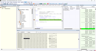
We are conducting an EMIF communication test by connecting TMS570LS3137 and FPGA.

This is a test that writes data from the FPGA when you try to read the address of the EMIF area in TMS570.

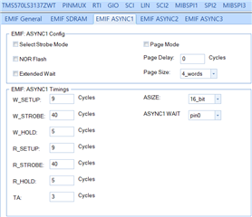
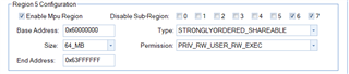
First, I briefly performed an EMIF Read/Write test on TMS570 as follows.
int fpga = FPGA_ADDR(0x00);
*(uint16 *)(fpga + 0x100) = 0x1234;
newTelegramMsg[0] = *(uint16 *)(fpga + 0x100);
The newTelegramMsg[0] value was read normally at 0x1234.

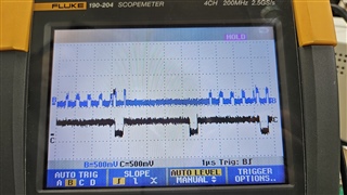
However, the EMIF test between TMS570 and FPGA did not work well.
In TMS570
newTelegramMsg[0] = *(uint16 *)(fpga + 0x100);
If you do something like the code above
The FPGA recognizes the CS and OE pins and loads data on the data line. When you read the data sent from the FPGA, values ​​like 0x40, 0x41... are read.

Is this a timing issue?
So what should we do?

Best Regards,
IBLEE

  • newTelegramMsg[0] = *(uint16 *)(fpga + 0x100);

    This is the oscilloscope waveform when this code is run.
    Black is the OE pin, blue is the Data pin.
    In any case, I ask whether garbage data should be read when OE goes from low to high.

  • Halcogen setting Value.

  • Memory settings are as shown in the picture above.

  • Hi IBLEE,

    I need the following things to understand it better:

    1. What exactly FPGA you are using, may i know the part number of it?

    2. Can you please share your complete project? If you need, you can send through private message as well.

    Black is the OE pin, blue is the Data pin.

    3. I don't understand which data pin, actually we should have 8 or 16 data lines right? but your waveform has only single data line? which data line it is?

    4. If possible, can i also get the connectivity diagram between FPGA and TMS570?

    --
    Thanks & regards,
    Jagadish.

  • Dear Jagadish.

    1. I'm sorry, but all I can tell you is the chip information used.
    - ARTIX-7 (XC7A200T)
    2. I cannot provide information because I am an outsourcing company. Sorry.
    3. This is line D2. Because there weren't that many probes, I only took a picture of one data line.
    4. The connection between TMS570 and FPGA is as follows.
    -EMIF_A0~A15
    -EMIF_D0~D15
    -EMIF_NCS[2]
    -EMIF_NWE
    -EMIF_NOE
    -EMIF_BA[1]

    Best Regards,
    IBLEE

  • Dear Jagadish

    I have a question. If you write 0x1234 to address 0x60000100 and look at the memory with dump, you will see values ​​0x40, 0x41, etc. that increase sequentially.

    Is this normal?

    Best Regards, 

    IBLEE

  • Hi IBLEE,

    I am not sure about the PLA logic used inside the FPGA. So, i don't know about what the output for should be reading the 0x00000100 address of FPGA.

    If it is a memory, then it should need to be read the same value what we write into it at corresponding location.

    --
    Thanks & Regards,
    Jagadish.

  • Dear Jagadish.

    I'm trying to communicate with the FPGA through the EMIF async area.
    newTelegramMsg[0] = *(uint16 *)(0x6000000+ 0x100);

    When I read data like this, the FPGA sends 2 bytes of data through the data line.

    Isn't it okay to do this?

    Best Regards,
    IBLEE

  • Hi IBLEE,

    When I read data like this, the FPGA sends 2 bytes of data through the data line.

    As we connected 16-bit data lines between FPGA and TMS570 right. So, we should get 16-bit data only.

    What do you mean by two bytes in your case, are you not receiving two bytes (16-bit data) on D0 to D15 data lines? 

    If you are receiving like this then its fine, as per my understanding.

    --
    Thanks & Regards,
    Jagadish.

  • Dear Jagadish.

    okay. I connected it like you said.
    I'm trying to receive data through D0~D15, but what I'm curious about here is that even if the FPGA sends data through D0~D15, the value at address 0x60000100 does not change to the value sent from the FPGA through the IDE's memory dump.
    The code I used is below.
    newTelegramMsg[0] = *(uint16 *)(0x6000000+ 0x100);

    The FPGA sent the value 0xffff through D0 to D15, but in fact, the newTelegramMsg[0] buffer contains 0x40, and the IDE's memory dump 0x60000100 also contains the value 0x40.

    If the FPGA sends the 0xffff value through D0 to D15, shouldn't the 0xffff value be displayed at 0x60000100 as well?

    Am I misunderstanding this?

    Best Regards,

    IBLEE

  • Hi IBLEE,

    Is it possible for you to setup one live debugging session. That would be very helpful for me to understand it well and can provide my suggestions to you.

    I will be available from 10AM to 7PM IST. If you are okay with it, we can have call on tomorrow.

    --
    Thanks & regards,
    Jagadish.

  • Dear Jagadish.

    Thank you so much for your proactive response.

    I think the live debugging you suggested would be a bit difficult because it doesn't overlap with my commute time.

    I went to work today and tested one more thing.
    The test board was DEVKIT and I used the same testing method as mentioned above.

    Then, the symptoms turned out to be different from the actual target board.

    In devkit, the data was updated well in memory at address 0x60000100.
    It doesn't work on the target board.
    I'm really confused.

    I checked to see if there was a difference in halcogen between the devkit and target board, and it looked the same to me.

    So is it a hardware connection issue? What's the problem?
    I think I need to think about it some more.

    Best Regards,

    IBLEE

  • This picture is from when testing on the target board.

    Best Regards,

    IBLEE

  • Hi IBLEE,

    I think this is expected behavior only.

    Before explaining why, i want to clarify one more thing that is, how the data in the memory browser in the CCS is displaying for EMIF region.

    For below highlighted emif region, there won't be any physical memory inside the controller:

    If we trying to access this region, in the background EMIF communication will takes place to get the data in the corresponding region.

    So, in the similar way if you trying to access the 0x60000100 region from memory browser of CCS, in the background JTAG will send commands to the processor and in the background, it will read the data using EMIF.

    So now come to the why we are reading all 0's in DEV kit is, because in DEV Kit there is no EMIF slave connected for connected for CS2. I mean no asynchronous memory or FPGA was there in this region like what you have in your target board.

    So, if CCS trying to display this region as there is no slave memory connected to it right, so the data lines might give all zeros while EMIF communication takes place. That is the reason we are getting all zeros for this region in DEV KIT.

    However, in your target board you have FPGA for this region right. So, if CCS memory browser access this region in the background EMIF communication will takes place in the controller and we will get the data from FPGA.

    The data 0x40, 0x41 ... etc., all these data are from FPGA only. If you ask me why this data is received from FPGA, then i don't know why because it is depending on the logic used inside the FPGA. You should need to check the FPGA logic used inside the FPGA to understand why you are getting this data.

    --
    Thanks & regards,
    Jagadish.

  • Dear Jagadish.

    thank you so much.
    I understand what you mean.
    I'll try more and ask again if I have any questions.

    Best Regards,
    IBLEE

  • IBLEE,

    I understand what you mean.

    Good to hear that!

    I'll try more and ask again if I have any questions.

    Sure.

    --
    Thanks & regards,
    Jagadish.

  • Dear Jagadish.

    I am currently connecting and using multiple PCBs on the target board, but a HW problem related to EMIF communication was discovered.

    Thank you for thinking about it with me and explaining it to me.

    First, I'll try again once the HW is fixed, and if I have any questions, I'll ask again.

    Best Regards,

    IBLEE