Part Number: MSP-EXP432E401Y
Other Parts Discussed in Thread: TPS2052B, DRA829
Tool/software:
Hi,
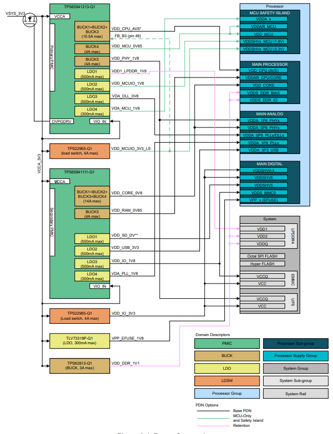
I use the board MSP-EXP432E401Y to program NVM on PMIC TPS65941213 and TPS65941111(SCH is the same as TI PROC112A but VCCA is 5.0V).
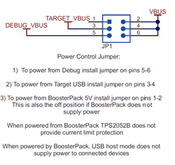
For convenience, I short PIN3 and PIN5 on JP1, and program TPS65941111 successful on GUI.
But after this, I can not program the PMIC again and I find the COM on my computer is disappear.
I re plug and unplug the USB(the power is down and on again), and I still can not see the COM on my computer.
Then I download MSP-EXP432E401Y again, I only see "Stellaris Device Firmware Upgrade" on my computer.
I download blinky_MSP_EXP432E401Y_nortos_ccs.projectspec in simplelink_msp432e4_sdk_4_20_00_12, than I find the code run normally and can run one-step mode, but the PIN state is error.
No mater the code set the PIN PN0 high or low, the voltage of the PIN PN0 is 0.8V,
When I change the code to set PIN PN1, and the voltage of PIN PN1 is still 1.7V(on one-step mode to set the PIN high or low).
By this I am sure the chip MSP432 on the MSP-EXP432E401Y is breakdown.
I want to know is there any wrong with short PIN3 and PIN5 on JP1?
How can I repair the board? Return the board to the factory or buy a new chip for replacement?
Thanks.