This thread has been locked.

If you have a related question, please click the "Ask a related question" button in the top right corner. The newly created question will be automatically linked to this question.

AM2431: Controlling Multiple GPIO in Single API Call

Part Number: AM2431

Tool/software:

I looked through the TRM and understand GPIO can be controlled with registers at baseAddr = 0x00600000 (GPIO0)
After GPIO are configured for input/output/PU/PD/etc...you can write GPIO_SET_DATAyy register to define which bits are H/L in a bank.
With the above register write, it is possible to set multiple GPIO pins H/L in a single instruction.

Apologize for not digging through the header files yet,
but I was just wondering if the GPIO API also supported setting multiple GPIO with a single API function call? For example...

GPIO_pinWriteHigh(baseAddr, 0b0011);

Is something like this possible, or does the register write need to be used?

  • Hello Keito,

    Thanks for your query.

    I was just wondering if the GPIO API also supported setting multiple GPIO with a single API function call?

    Unfortunately, There are no APIs to write multiple GPIO pins at once. The only option to write multiple GPIO pins High/Low is to directly write the register values.

    Note - Only 2 consecutive GPIO Bank (i.e.32 GPIO) pins can be written at once. The GPIO banks register that can be written at once are in following pair - [01, 23, 45].

    Hope the above information helps.

    Regards,

    Tushar

  • Also, I was wondering about the banks and GPIO numbering.

    Table 5-41 and Table 5-42 list the GPIOs.
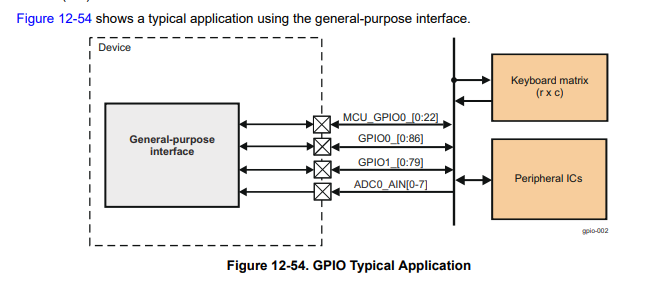
    GPIO0 has 87 gpio pins.
    GPIO1 has 80 gpio pins.

    The TRM (Section 1.3.9) states the GPIO instances have 9 Banks with 16x GPIO each.

    The GPIO registers in the TRM show each of the 9 Banks can be controlled (i.e. GPIO_SET_DATAyy can set pins in each bank)

    What I don't understand is the matching between banks and GPIO pin numbers.

    Is GPIO0 (baseAddr = 0x00600000) Bank 0 = GPIO0_0 ~ GPIO0_15?
    The datasheet (Table 5-41) states GPIO0_86 as the last GPIO0 gpio.

    Going with this understanding GPIO0_86 would be controlled by GPIO0 Bank 5?
    But that means Bank 6 ~ Bank 8 are unused?

    For GPIO1 (which only has up to GPIO0_79) this maxes out at GPIO1 Bank 4...

    Is this understanding correct?

  • Hi Keito,

    Table 5-41 and Table 5-42 list the GPIOs.
    GPIO0 has 87 gpio pins.
    GPIO1 has 80 gpio pins.

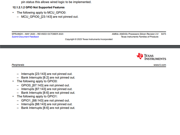
    Please refer to the section 12.1.2.1.2 GPIO Not Supported Features of the TRM to see what features are not supported by GPIO.

    As you can see from the below screenshot GPIO0_[87:143] are not pinned out. Similarly for GPIO1_[88:143] pins are not pinned out.

    Please refer below screenshot.

    For GPIO1 (which only has up to GPIO0_79) this maxes out at GPIO1 Bank 4...

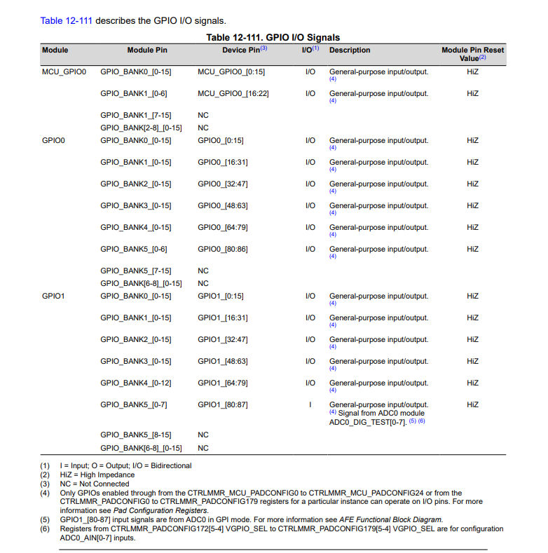
    Yes, the above details are correct. The GPIO1_[80:87] pins are configured as ADC and cannot be used in GPIO mode. This pins can only be used in GPI mode.

    Going with this understanding GPIO0_86 would be controlled by GPIO0 Bank 5?
    But that means Bank 6 ~ Bank 8 are unused?

    Please refer below screenshot for GPIO signals details.

    Hope the above information helps.

    Regards,

    Tushar

  • Hi Tushar,

    Perfect; I have an idea how to move forward now. Thanks!

  • Hi Keito,

    Perfect; I have an idea how to move forward now.

    Thanks for the confirmation. 

    Happy to help Slight smile

    Regards,

    Tushar