


Tool/software:
SAP Part number S4MF06607BSPZQQ1
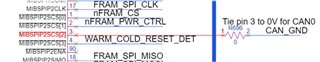
Due to a coding error, pins 3 MIBSPIP2SCS[2] and 4 MIBSPIP2SCS[3] are NOT designated as input (as intended) but assert OUTPUT HIGH leading to contention with the circuitry fitted to the PCB as follows:
Pin 3 is tied to ground through a zero ohm resistor. However shortly after power-up PIN3 is commanded high for ~0.55ms
When the 0R resistor is replaced with 100R in order to measure pin output current the following was recorded:
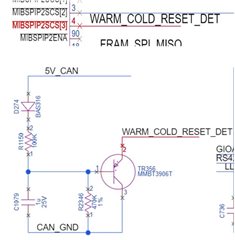
Pin 4 is configured thus:
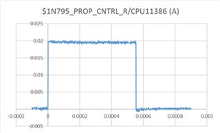
The circuit was modified with a 10R resistor in series with TR356 collector (pin3 ) in order to measure the current.
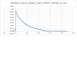
At power-on the measure current is shown below. Pin4 is asserted high shortly after power up. Current peaks at around 40mA then reduces as C1079 charges up.
The TMS470 data sheet specifies output currents(s) as 4mA (Adaptive Impedances 4mA buffer), so we recognise that we are operating outside of the datasheet limits during this brief transient period. However over 100's of power on cycles we have not seen any failures.
Q1. Can you provide any further information on the current capability of these pins?
Q2. If we have stressed these pins, would any stress be limited to these pins only or would the whole device now be considered as "over-stressed"?
Any advise you can offer is gratefully received.

