This thread has been locked.

If you have a related question, please click the "Ask a related question" button in the top right corner. The newly created question will be automatically linked to this question.

MSPM0G3507: All ADC values are 0x0000

Part Number: MSPM0G3507
Other Parts Discussed in Thread: SYSCONFIG, , LM4040

Tool/software:

Similar to other threads, i'm only getting 0x0000 returned.

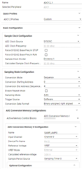
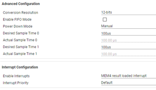
I've set the powerdown mode to manual and lengthened the sampling period.

    SYSCFG_DL_init();
    NVIC_EnableIRQ(ADC12_0_INST_INT_IRQN);
    NVIC_EnableIRQ(ADC12_1_INST_INT_IRQN);

    forever(

        DL_ADC12_enableConversions(ADC12_1_INST); //??? is this needed a 2nd time after each conversion?  wasn't getting a 2nd conversion so added
        DL_ADC12_startConversion(ADC12_1_INST);

        gStateAdc[1] = adcBusy;

        while(gStateAdc[1]!=adcComplete) <wait>

        //should not be able to get to this point until after interrupt: DL_ADC12_IIDX_MEM4_RESULT_LOADED

         for(uint16_t delay=0;delay<0xF000;delay++) __NOP(); //this is debug code since Janz Bai questioned if there was enough time passed to get any values.

        gRegSpace[REG_AdcAmp0] = DL_ADC12_getMemResult(ADC12_1_INST, DL_ADC12_MEM_IDX_0);
        gRegSpace[REG_AdcAmp1] = DL_ADC12_getMemResult(ADC12_1_INST, DL_ADC12_MEM_IDX_1);
        gRegSpace[REG_AdcAmp2] = DL_ADC12_getMemResult(ADC12_1_INST, DL_ADC12_MEM_IDX_2);
        gRegSpace[REG_AdcAmp3] = DL_ADC12_getMemResult(ADC12_1_INST, DL_ADC12_MEM_IDX_3);
        gRegSpace[REG_Adc48v ] = DL_ADC12_getMemResult(ADC12_1_INST, DL_ADC12_MEM_IDX_4);

        <wait for 100ms timer>

    )

void ADC12_1_INST_IRQHandler(void)
{
    DL_ADC12_IIDX pendingInterrupt = DL_ADC12_getPendingInterrupt(ADC12_1_INST);
    switch (pendingInterrupt) {
        case DL_ADC12_IIDX_MEM4_RESULT_LOADED:
            //DL_ADC12_stopConversion(ADC12_1_INST);
            //DL_ADC12_disableConversions(ADC12_1_INST);
            gStateAdc[1] = adcComplete; //change state after stopping conversion
            break;
}

I do get interrupts, but every conversion including the first one is value 0x0000

  • Hello,

    I will reply to you tomorrow.

    Best Regards,

    Janz Bai

  • Hello,

    There are some important points I want to share with you: 

    1). If you set "trigger source" to "software", you should use the ”startConversion“ instruction when you want to do ADC conversion, such as using timer and  periodically start conversion in timer interrupt.

    2). If you don't want to use the timer interrupt but you want to use the timer for periodically conversion, you should set "trigger source" to "event" and do related configuration on Sysconfig. 

    3). If you don't click the "Enable Repeat Mode" on Sysconfig, you should call the "enable_Conversions" instruction before you want to do ADC conversion.

    4). I think the main cause about your issue is that you don't give ADC enough time to do sampling and conversion before you read the results. In your code, you immediately read the ADC memory after you "start conversion" which will cause you read the 0x0 out from ADC memory.

    5). You can download our SDK from ti.com. And you can find the example project: "adc12_triggered_by_timer_event_LP_MSPM0L3507" in the SDK. You can refer to this example and related part (Chapter ADC) in our technical reference manual which can be downloaded from ti.com for detailed information. 

    Best Regards,

    Janz Bai

  • I have the SDK, i modeled my code after the example you provided.  though the example was not reoccurring, the comment in my code indicates that i figured out that i needed to DL_ADC12_enableConversions(ADC12_1_INST) in order to get a 2nd conversion.

    I apologize that my initial code i pasted in was not complete, i hadn't noticed i removed too much.  i've fixed the original post
    the line:
    "while("

    should have been

    "while( gStateAdc[1] != adcComplete ) wait"

    in addition i didn't explicitly show the line, but i also do set gStateAdc[1] = adcBusy after i start the conversion.

    i've stepped through my code and it seems like things are setup and working properly.

    so answering your points:
    1) yes, its in my code
    2) this is not the mode i chose
    3) yes, its in my code
    4) since i can't see delays when stepping through my code as an experiment i waited until after i receive DL_ADC12_IIDX_MEM4_RESULT_LOADED and then in addition i do:
        for(uint16_t delay=0;delay<0xF000;delay++){
            __NOP();
        }
    even with this extra delay i still see 0x0000
    5) yes, i designed my code on this and many other examples

    i didn't want to upload my whole source publicly, but if you want to look at my code i can share it privately.

    I reviewed the syscfg and modified the clock from sysosc to ulpclk like in the example, but that didnt change behavior

  • Hello,

    1). Yes, you do need the "enable_Conversions" to do second conversion because after completing once conversion, the ADC will be "disable conversion".

    2). I think you can modify the "while(gStateAdc[1]!=adcComplete) <wait>" to "while (gStateAdc[1]!=adcComplete) {__WFI()}" which will help you save power even though this is not the cause of your issue.

    3). Can you directly download the example code from SDK into your M0? If do this, can you see the correct result of ADC?

    4). Maybe you need also check whether your signal is too small to be sampling.

    Best Regards,

    Janz Bai

  • 1) yes, that was in the code when i first started the ticket.  i had figured it out.  thank you for verifying that it was nessesary.

    2) my code is more complex, i have both adc channels reading 5 pins.  i also have an spi peripheral running.  i only transfer the adc values into registers when not in the middle of a protocol transaction... i think i could put in a WFI when none of these things are occuring, but i'll worry about that once everything is working.  thanks for the suggestion.

    3) yes, i get some values.  i started checking what is different, from general setup there was the clock difference which i changed.  otherwise i didn't see what was functionally different, but i could have overlooked something.  i was going to start from the reference and start making changes step by step until it matches my design.  i haven't been able to do that yet due to other obligations, i hoped that you might have some insight before i could get back to it. 

    I already had to do this once as i could not get my interrupt routines to connect (kept getting default handler, so i had to start from a super basic design and add in parts step by step until i had recreated my design and the functions worked)

    4) i'm using a 3V external reference that appears correct.  some of the signals are on the order of 2.3V

  • Hello,

    From your configuration of ADC part, I didn't find error currently. Because your code is more complex, I think doing more debugging using debugger is also a good way to find the root cause. And when you debug it, please pay attention to the clock usage and peripheral usage in different power mode, you can refer to the Table 2-1 in our G series Technical Reference Manual. 

    And there are two methods to do simply tests: 1). Just configurate the ADC part as you mentioned in this post without configuration any other no-related peripherals (test ADC module separately) and check whether you can get correct value. 2). Try to move the ADC module from example code into your own code directly and check whether you can get correct value.

    Anyway, the Technical reference manual can give you much help: MSPM0 G-Series 80-MHz Microcontrollers Technical Reference Manual (Rev. A) (ti.com)

    Best Regards,

    Janz Bai

  • I've traced the issue to trying to use VREF.

    using the sample code, i turned 2-ADC with 5 ch each, i still got values.

    then i added

    and modified 2 of the ch

    after doing this the 2 channels i changed read back 0 when they did not before.

    is there something else i need to do to make this work?  can you test on one of your boards?

  • Hello,

    So you mean that you "using the sample code, i turned 2-ADC with 5 ch each, i still got values", but when you added the VREF module into your code and modify the reference of ADC channel 0 & 1 from VDDA to VREF, without other modification, you find that the results are 0x0, right ?

    Can you check whether there is a decoupling capacitor on the reference pins? And you can double check with this:

    Hope this information can help you to do debug work.

    Best Regards,

    Janz Bai

  • in my design, if i only change channels to use VDDA instead of VREF i get values for those channels.

    there is a reference design adc12_single_conversion_vref_external
    this shows me the same results (i only changed the package, and the adc channel to use the internal supply, and the voltage setting of vref.


    regarding my external vref, I have 2.2U to reduce noise on the reference and a 0402 1UF bypass cap close to the micro.

    when i use a multimeter, i see that it is very close to 3.0V

    my vdd is 3.3V

    some values sampled are close to 0, some 2.5V, plus measuring internal temp and vcore show the same behaviours.

    as described in other threads, it is not expected that even a 0V signal will read back 0x0000 as there is noise and offset.

    can you verify that the reference works?  even if you dont have a real reference, maybe you could tie the pin of vref to a different pin and output 3.3V... its not a clean reference, but its a voltage that could be used to test?

  • a couple of related questions of additional questions

    1)
    Where do i find the documentation on all of the internal register definitions, the registers and what each bit does?

    2)
    I see SYSCFG_DL_VREF_init()

    as part of SYSCFG_DL_init()

    i dont see any other of the DL_VREF called in the adc12_single_conversion_vref_external sample.  do i need to call any other functions before use?

    3)

    what values should be in the vref registers when using external reference?

    vref            
        VREF_GPRCM            
        VREF_CLKDIV    0x00000000    Clock Divider [Memory Mapped]    
        VREF_CLKSEL    0x00000000    Clock Selection [Memory Mapped]    
        VREF_CTL0    0x00000000    Control 0 [Memory Mapped]    
        VREF_CTL1    0x00000000    Control 1 [Memory Mapped]    
        VREF_CTL2    0x00000000    Control 2 [Memory Mapped]    

  • Hello,

    About current issue, please let me to summary it: 

    1). using the "adc12_triggered_by_timer_event_LP_MSPM0L3507" example code can work, but just modifying from VDDA to VREF can' work (read out 0x0)

    2). without any modifying, directly using the "adc12_single_conversion_vref_external" example code with external reference, can it work? Or it can't work unless you change the reference to internal ?(I am sorry I don't understand the "this shows me the same results(.. ...)", so please help me confirm it)

    3). It seems that the cause is the external VREF. And I will do some tests this week. 

    And about your additional questions: 

    1). I have sent you the link of TRM before, you can find the description and function of each register in it: MSPM0 G-Series 80-MHz Microcontrollers Technical Reference Manual (Rev. A) (ti.com). Please read it.

    2). You don't need to call other function because when you configurate the ADC and VREF part in Sysconfig, it has been cofigurated completely.

    3). Please refer to the TRM.

    Best Regards,

    Janz Bai

  • I'll start a new test and document steps and the result
    1) import adc12_single_conversion_vref_external_LP_MSPM0G3507_nortos_ticlang
    2) change package to VQFN-32 because thats whats on my board.
    3) modify VREF -> basic configuration -> External Voltage = 3.0V
    4) this code when i looked using the debugger would not show me the value of adcResult, i could look at the assembly and see which Core Registers were being used, but to make things more clear for this example i modified the code as follows:
    4a) added a volatile uint16_t gPrevAdcVal; outside of main
    4b) added gPrevAdcVal = adcResult;
    5) Debug Run
    6) pause and inspect values, gPrevAdcVal was 0x0000
    7) modify ADC12_0 -> ADC Conversion Memory Configurations -> ADC Conversion Memory 0 Configuration -> Reference Voltage = VDDA (was VREF)
    8) Build project, Debug, pause
    9) gPrevAdcVal = 0xBED

  • any update?  are you able to find a board with vref pin?  what behavior do you see?

    thanks.

  • Hello WorkBee,

    I have done some tests on my side using the example project: "adc12_single_conversion_vref_external" and MSPM0G3507 LaunchPad, and use a 3.3 V external source as the external reference. After I set up the 3.3 V source as the reference and the 1.1 V source as the input of ADC, I enter debug mode and I can get ADC result correctly which is not 0. This is the code I used. 

    adc12_single_conversion_vref_external_LP_MSPM0G3507_nortos_ticlang.zip

    I think that maybe you need to confirm that when your MCU is powered up and ADC starts to work, Your reference voltage has been stabled to 3 V (the value you used mentioned in previous reply).

    Best Regards,

    Janz Bai

  • I appreciate you looking into this.  i took your project, and after much fighting with CCS (ended up reinstalling everything) I am now running the same version software as you.

    the code ran on my launchpad, but didnt work correctly (i thin i t was all 0xFF, but this can be explained as my launchpad does not have an external voltage on the ref pin.)

    I then ran the code on my board (without changing the package type in sysconfig) I wasn't sure if it would work or if i needed to modify something... internally i assumed that it was setill using the same internal resources so it would still work.  i read back 0x0000

    i then changed the sysconfig to be the proper package, i read back 0x0000

    i double checked the datasheet, sysconfig, pinout, and looked verified with the pcb viewer,  the pin looks correct.

    i am looking a via right next to the part:


    multimeter says 2.997, diff prope on oscilliscope while running says 3.064-3.068

    on the off chance there was a solder issue, i opened a new board and am now testing on it.  i still see 0x0000.

    i have an earlier part, not sure if that matters...

    Mspm0
    G3507S
    TIX3688
    AL01 G4

    thank you for your continued support.

  • Hello WorkerBee,

    So you mean that using the example code which I sent to you can't work normally, and the result you read back is still 0x0? It is very stranger. And in my previous reply, I mentioned that you must confirm that when ADC starts to work, your external reference must by stable because if not, ADC may calculate the result based on the wrong reference voltage value. And another point about it is the cap you used near the VREF. On our LaunchPad, the cap between the VREF+ and VREF- is about 1 uF. In our datasheet, it mentioned that when you use the external reference, a cap value should be selected based on the source value. But maybe the Cap you used is a little big.

    Best Regards,

    Janz Bai

  • I can elaborate on my previous
    "diff prope on oscilliscope while running says 3.064-3.068"
    Using the sample code which periodically samples the channel (vref in use)

    i use a differential probe, using peak detect aquisition mode to catch any glitches in the signal.

    i turned the trigger voltage as low as possible until i barely got any triggers, meaning i was getting the worst case waveform.

    as you can see its very close to 3.0V

    even if the signal was not super stable i fail to see how it could result in a 0x0000 reading.  if the reference is too low then i would expect the value captured to be artificially high... like on my launchpad where i dont have a vref, it read back max value.

    in addition too much capacitance for an external ref, i dont think that this is a concern for the microcontroller as it's only using this voltage, not trying to regulate it.  the capacitance is required to smooth out any current spikes, and any problems with capacitance would be on the device regulating the voltage, in this case the LM4040 which states:
    "The LM4040 does not require an output capacitor across cathode and anode for stability. However, if an output bypass capacitor is desired, the LM4040 is designed to be stable with all capacitive loads"

    and again, if this was a problem, i still would not expect the value to be "0x0000" i would expect a value too high.

    on a different ADC question, the TI response was that they did not expect the value to be 0x0000 as even a 0 voltage signal would have some non zero value.

    I've contacted my FAE and linked them to this thread.  do you have any other ideas?

  • Hello WorkerBee,

    Please let me do a summary:

    1). I can get correct value using the example code which is sent by me;

    2). You can't get the correct value using the example code which is sent by me, always 0x0h;

    3). But you can get the correct value when you change the reference value from external to VDDA;

    And can you do a simply test using the MSPM0G3507 LaunchPad with the external reference to check whether you can get the correct value when you add external reference on LaunchPad.

    It is a good idea to contact our FAE, it may need FAE to check your hardware circuit. It seems that the root cause maybe the hardware.

    Hope you can resolve this issue and have a nice working day

    Best Regards,

    Janz Bai