This thread has been locked.

If you have a related question, please click the "Ask a related question" button in the top right corner. The newly created question will be automatically linked to this question.

TM4C1294KCPDT: How to set flash mirror mode in TM4C1294KCPDT

Part Number: TM4C1294KCPDT
Other Parts Discussed in Thread: TM4C1294NCPDT

Tool/software:

Hi experts,

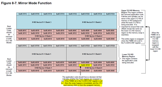
My customer wants to configure flash mirror mode using TM4C1294KCPDT.

some E2E link say that TM4C1294KCPDT does not work in mirror mode.

https://e2e.ti.com/support/microcontrollers/arm-based-microcontrollers-group/arm-based-microcontrollers/f/arm-based-microcontrollers-forum/498393/flash-mirror-mode

Please let me know the exact and detailed mirror mode switching sequence including the example source.

thanks 

regards

  • Hi Robin,

      As confirmed by Amit in the post you refer, mirror mode is not available on devices with 512kB of flash which is TM4C1294KCPDT. You would need to use parts with 1MB flash such as TM4C1294NCPDT. As far as the switching sequence, you can find the instructions in the datasheet or the post has the example code provided by the customer. A swap will take effect by writing to the FMME bit in the FLASHCONF register.

    8.2.3.3 Flash Mirror Mode
    Flash mirroring allows multiple copies of software to exist in Flash simultaneously. The software
    can run from the lower banks at the same time software is updating a mirrored copy on the upper
    bank. In addition to the data, the boot loader in both the lower and upper banks must be mirrored

    while programming the flash contents. If data needs to be recovered, a hot swap can be done by
    setting the FMME bit in the FLASHCONF register banks are idle during the swap.
    The prefetch buffers must be invalidated during the execution of a hot swap. Next, the address
    translation logic decodes up to 512 KB from the upper banks to the lower banks. Once the banks
    are swapped, the mirrored flash image is then used. The address translation logic translates the
    address to the upper banks until the next swap. Figure 8-7 on page 609 depicts the configuration
    necessary when executing Flash mirroring.


    Note: After a mirror mode has been executed and the code locations have been swapped from
    the upper memory banks to the lower, the application can continue to read from the lower
    memory bank address locations. However, when erasing or programming the swapped
    memory, the application must use the "real" upper memory address of the code before it
    was swapped. For example, in Figure 8-7 on page 609, when the yellow highlighted location
    0x00.3FE8 is swapped with 0x08.3FE8 the application's next read location is 0x00.3FEC.
    However, if the application were to program or erase the next location it would need to write
    or erase location 0x08.3FEC.