This thread has been locked.

If you have a related question, please click the "Ask a related question" button in the top right corner. The newly created question will be automatically linked to this question.

MSPM0L1306: DAC peripherals output non-linear

Part Number: MSPM0L1306
Other Parts Discussed in Thread: SYSCONFIG

Tool/software:

Hi team,

My account is evaluating MSPM0L1306 DAC but it seems like the DAC output is not linear.

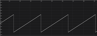
When the setting value is the upper limit. As shown as figure below, the linearity is lost.

※The figure below shows the repeated output of the DAC output as "0 → 1 →~→ 254 → 255 → 0 → 1 → ~"


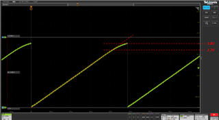
Can this be judged to be the ability of microcontrollers? Or is there a possibility improve it by settings?


Thank you,

Kenley

  • Hi Kenley,

    What is the reference for DAC? Did the customer use the VDDA as reference? Are they using the example code to test directly?

  • How are you sampling the DAC8 output? Datasheet (SLASEX0D) Table 7.17.1 seems to say that OPA can only handle up to (VDD-0.3) even in the best case.

  • Hi Zhao-san and Bruce,

    Thank you for your support.

    Let me share all the information from customer.

    Project File: 

    MSPM0Lxx_Driver.c
    #include "MSPM0Lxx_Driver.h"
    
    
    //*****************************************************************************
    // detection module power init
    //*****************************************************************************
    void Driver_DetectionPowerEnable(void)
    {
        DL_ADC12_reset(ADC12_INST);
        DL_VREF_reset(VREF);
        DL_COMP_reset(COMP0);
        DL_OPA_reset(OPA0);
        DL_OPA_reset(OPA1);
        DL_ADC12_enablePower(ADC12_INST);
        DL_VREF_enablePower(VREF);
        DL_COMP_enablePower(COMP0);
        DL_OPA_enablePower(OPA0);
        DL_OPA_enablePower(OPA1);
        delay_cycles(POWER_STARTUP_DELAY);
    }
    void Driver_DetectionPowerDisable(void)
    {
        DL_ADC12_disablePower(ADC12_INST);
        DL_VREF_disablePower(VREF);
        DL_COMP_disablePower(COMP0);
        DL_OPA_disablePower(OPA0);
        DL_OPA_disablePower(OPA1);
    }
    
    //*****************************************************************************
    // Vref Init
    //*****************************************************************************
    static const DL_VREF_Config gVREFConfig = {
        .bufConfig      = DL_VREF_BUFCONFIG_OUTPUT_1_4V,
        .holdCycleCount = DL_VREF_HOLD_MIN,
        .shCycleCount   = DL_VREF_SH_MIN,
        .shModeEnable   = DL_VREF_SHMODE_DISABLE,
        .vrefEnable     = DL_VREF_ENABLE_ENABLE,
    };
    static const DL_VREF_ClockConfig gVREFClockConfig = {
        .clockSel    = DL_VREF_CLOCK_BUSCLK,
        //.clockSel    = DL_VREF_CLOCK_MFCLK,
        .divideRatio = DL_VREF_CLOCK_DIVIDE_1,
    };
    
    void Driver_VrefInit(void)
    {
        DL_VREF_setClockConfig(VREF, (DL_VREF_ClockConfig *) &gVREFClockConfig);
        DL_VREF_configReference(VREF, (DL_VREF_Config *) &gVREFConfig);
        while (DL_VREF_CTL1_READY_NOTRDY == DL_VREF_getStatus(VREF))
            ;
    }
    
    
    //*****************************************************************************
    // ADC Init and sampling
    // Use software averaging to increase resolution
    // ADC 1 sampling time: 1us*SAMPLE_TIME + 0.5us conversion time + code run time(21us)
    // ADC sampling total time:ADC 1 sampling time * ADC_AVERAGE_TIMES
    //*****************************************************************************
     volatile bool gCheckADC;
     uint16_t gADCSamples[ADC_AVERAGE_TIMES];
     static const DL_DMA_Config gDMA_CH0Config = {
         .transferMode   = DL_DMA_SINGLE_TRANSFER_MODE,
         .extendedMode   = DL_DMA_NORMAL_MODE,
         .destIncrement  = DL_DMA_ADDR_INCREMENT,
         .srcIncrement   = DL_DMA_ADDR_UNCHANGED,
         .destWidth      = DL_DMA_WIDTH_WORD,
         .srcWidth       = DL_DMA_WIDTH_WORD,
         .trigger        = DMA_ADC0_EVT_GEN_BD_TRIG
     };
    
     /* ADC12_0 Initialization */
     static const DL_ADC12_ClockConfig gADC12_0ClockConfig = {
         .clockSel       = DL_ADC12_CLOCK_SYSOSC,
         .divideRatio    = DL_ADC12_CLOCK_DIVIDE_8, //Select suitable clock divide ratio
         .freqRange      = DL_ADC12_CLOCK_FREQ_RANGE_24_TO_32,
     };
    
     _iq5 Driver_ADCInitAndSampling(uint32_t adcChannel, uint32_t vrefSource, _iq5 iq5AdcOffset)
    {
    #ifdef TEST
         _iq5 iq5Temp,  iq5Temp1;
         _iq5 iq5SquareSum=_IQ5(0);
    #endif
        _iq5 iq5AdcConvResult;
        uint32_t u32AdcSum = 0;
        uint16_t u16Counter;
        uint16_t u16AdcResult;
    
        gCheckADC = false;
        DL_ADC12_reset(ADC12_INST);
        DL_ADC12_enablePower(ADC12_INST);
        DL_ADC12_setClockConfig(ADC12_INST, (DL_ADC12_ClockConfig *) &gADC12_0ClockConfig);
        DL_ADC12_initSingleSample(ADC12_INST,
           DL_ADC12_REPEAT_MODE_ENABLED, DL_ADC12_SAMPLING_SOURCE_AUTO, DL_ADC12_TRIG_SRC_SOFTWARE,
           DL_ADC12_SAMP_CONV_RES_12_BIT, DL_ADC12_SAMP_CONV_DATA_FORMAT_UNSIGNED);
        DL_ADC12_configConversionMem(ADC12_INST, DL_ADC12_MEM_IDX_0,
                                     adcChannel, vrefSource,
        DL_ADC12_SAMPLE_TIMER_SOURCE_SCOMP0, DL_ADC12_AVERAGING_MODE_DISABLED,
        DL_ADC12_BURN_OUT_SOURCE_DISABLED, DL_ADC12_TRIGGER_MODE_AUTO_NEXT,
        DL_ADC12_WINDOWS_COMP_MODE_DISABLED);
        DL_ADC12_enableFIFO(ADC12_INST);
        DL_ADC12_setPowerDownMode(ADC12_INST,DL_ADC12_POWER_DOWN_MODE_MANUAL);
        DL_ADC12_setSampleTime0(ADC12_INST,ADC_SAMPLE_TIME);
        DL_ADC12_enableDMA(ADC12_INST);
        DL_ADC12_setDMASamplesCnt(ADC12_INST,1);
        DL_ADC12_enableDMATrigger(ADC12_INST,(DL_ADC12_DMA_MEM1_RESULT_LOADED));
        /* Enable ADC12 interrupt */
        DL_ADC12_clearInterruptStatus(ADC12_INST,(DL_ADC12_INTERRUPT_DMA_DONE));
        DL_ADC12_enableInterrupt(ADC12_INST,(DL_ADC12_INTERRUPT_DMA_DONE));
        DL_ADC12_enableConversions(ADC12_INST);
    
        DL_DMA_initChannel(DMA, DMA_CH0_SEL , (DL_DMA_Config *) &gDMA_CH0Config);
        /* Configure DMA source, destination and size */
        DL_DMA_setSrcAddr(DMA, DMA_CH0_SEL,
          (uint32_t) DL_ADC12_getFIFOAddress(ADC12_INST));
        DL_DMA_setDestAddr(DMA, DMA_CH0_SEL, (uint32_t) &gADCSamples[0]);
          DL_DMA_setTransferSize(DMA, DMA_CH0_SEL, ADC_AVERAGE_TIMES>>1);
    
        DL_DMA_enableChannel(DMA, DMA_CH0_SEL);
    
        /* Setup interrupts on device */
        NVIC_EnableIRQ(ADC12_INST_INT_IRQN);
    
    //    DL_GPIO_clearPins(GPIOA,GPIO_UART0_TX_PIN);
        DL_ADC12_enableConversions(ADC12_INST);
        DL_ADC12_startConversion(ADC12_INST);
    
        while (false == gCheckADC) {
            __WFE();
        }
    //    DL_GPIO_setPins(GPIOA,GPIO_UART0_TX_PIN);
        for(u16Counter = 0;  u16Counter < ADC_AVERAGE_TIMES; u16Counter++)
        {
          u32AdcSum += gADCSamples[u16Counter];
        }
        iq5AdcConvResult =_IQ5div( _IQ5(u32AdcSum),_IQ5(ADC_AVERAGE_TIMES));
    
    #ifdef TEST
        for(u16Counter = 0;  u16Counter < ADC_AVERAGE_TIMES; u16Counter++)
        {
            iq5Temp = iq5AdcConvResult- _IQ5(gADCSamples[u16Counter]);
            iq5SquareSum += _IQ5mpy(iq5Temp,iq5Temp);
        }
        iq5Temp1 = _IQ5div( iq5SquareSum,_IQ5(ADC_AVERAGE_TIMES));
        //    Driver_Uart1TxU16Data(_IQ5int(_IQ5mpy(iq5AdcConvResult+iq5AdcOffset,_IQ5(10))));
        Driver_Uart1TxU16Data(_IQ5int(iq5AdcConvResult+iq5AdcOffset));
        Driver_Uart1TxU16Data(_IQ5int(_IQ5mpy(iq5Temp1,_IQ5(10))));
    #endif
    
    
        return (iq5AdcConvResult+iq5AdcOffset);
    }
    
    void ADC12_INST_IRQHandler(void)
    {
     switch (DL_ADC12_getPendingInterrupt(ADC12_INST)) {
         case DL_ADC12_IIDX_DMA_DONE:
             gCheckADC = true;
             break;
         default:
             break;
     }
    }
    //*****************************************************************************
    // 8bit DAC Init
    //*****************************************************************************
    static const DL_COMP_Config gCOMP_INSTConfig = {
        .channelEnable = DL_COMP_ENABLE_CHANNEL_NONE,
        .mode          = DL_COMP_MODE_FAST,
        .negChannel    = DL_COMP_IMSEL_CHANNEL_0,
        .posChannel    = DL_COMP_IPSEL_CHANNEL_0,
        .hysteresis    = DL_COMP_HYSTERESIS_20,
        .polarity      = DL_COMP_POLARITY_NON_INV};
    
    static const DL_COMP_RefVoltageConfig gCOMP_INSTVRefConfig = {
        .mode           = DL_COMP_REF_MODE_STATIC,
       .source         = COMP_CTL2_REFSRC_VDDA_DAC,
        .terminalSelect = DL_COMP_REF_TERMINAL_SELECT_NEG,
        .controlSelect  = DL_COMP_DAC_CONTROL_SW,
        .inputSelect    = DL_COMP_DAC_INPUT_DACCODE0};
    void Driver_DACInit(uint32_t u32DacValue)
    {
    #ifdef WORK_AROUND
        DL_SYSCTL_setVBOOSTConfig(DL_SYSCTL_VBOOST_ONALWAYS);
        DL_SYSCTL_enableMFCLK();
    #endif
        DL_COMP_init(COMP0, (DL_COMP_Config *) &gCOMP_INSTConfig);
        DL_COMP_refVoltageInit(
                COMP0, (DL_COMP_RefVoltageConfig *) &gCOMP_INSTVRefConfig);
    //    DL_COMP_setDACCode0(COMP0, COMP_INST_DACCODE0);
    
        DL_COMP_setDACCode0(COMP0, u32DacValue);
        DL_COMP_enable(COMP0);
    }
    
    //*****************************************************************************
    // OPA0 (used as a buffer) Init
    //*****************************************************************************
    static const DL_OPA_Config gOPA0Config0 = {
          .choppingMode   = DL_OPA_CHOPPING_MODE_DISABLE,
        .outputPinState = DL_OPA_OUTPUT_PIN_ENABLED,
        .pselChannel    = DL_OPA_PSEL_DAC8_OUT,
        .nselChannel    = DL_OPA_NSEL_RTOP,
        .mselChannel    = DL_OPA_MSEL_OPEN,
        .gain           = DL_OPA_GAIN_N0_P1,
    };
    void Driver_OPA0Init(void)
    {
        //__PG1_0_WORKAROUND__
        DL_SYSCTL_setVBOOSTConfig(DL_SYSCTL_VBOOST_ONALWAYS);
        //__PG1_0_WORKAROUND_END__
        DL_SYSCTL_enableMFCLK();
    
        DL_OPA_enableRailToRailInput(OPA0); //In order to input DAC= VCC
        DL_OPA_setGainBandwidth(OPA0, DL_OPA_GBW_HIGH);
        DL_OPA_init(OPA0, (DL_OPA_Config *) &gOPA0Config0);
        DL_OPA_enable(OPA0);
    }
    
    //*****************************************************************************
    // OPA1 (used as a buffer) Init
    //*****************************************************************************
     DL_OPA_Config gOPA1Config0 = {
          .choppingMode   = DL_OPA_CHOPPING_MODE_STANDARD,
        .outputPinState = DL_OPA_OUTPUT_PIN_ENABLED,
        .pselChannel    = DL_OPA_PSEL_IN0_POS,
        .nselChannel    = DL_OPA_NSEL_RTAP,
        .mselChannel    = DL_OPA_MSEL_IN1_NEG,
    };
    void Driver_OPA1Init(uint32_t u32Gain)
    {
        //__PG1_0_WORKAROUND__
        DL_SYSCTL_setVBOOSTConfig(DL_SYSCTL_VBOOST_ONALWAYS);
        //__PG1_0_WORKAROUND_END__
        DL_SYSCTL_enableMFCLK();
    
        gOPA1Config0.gain = u32Gain;
        DL_OPA_disableRailToRailInput(OPA1);
        DL_OPA_setGainBandwidth(OPA1, DL_OPA_GBW_HIGH);
        DL_OPA_init(OPA1, (DL_OPA_Config *) &gOPA1Config0);
        DL_OPA_enable(OPA1);
    }
    
    //*****************************************************************************
    // I2C control
    //*****************************************************************************
    static const DL_I2C_ClockConfig gI2C_INSTClockConfig = {
        .clockSel = DL_I2C_CLOCK_BUSCLK, .divideRatio = DL_I2C_CLOCK_DIVIDE_1};
    
    void Driver_I2cInit(void)
    {
        DL_I2C_reset(I2C_INST);
        DL_I2C_enablePower(I2C_INST);
    
        DL_GPIO_initPeripheralInputFunctionFeatures(GPIO_IOMUX_I2C_SDA,
                GPIO_IOMUX_I2C_SDA_FUNCTION, DL_GPIO_INVERSION_DISABLE,
                DL_GPIO_RESISTOR_PULL_UP, DL_GPIO_HYSTERESIS_DISABLE,
                DL_GPIO_WAKEUP_DISABLE);
        DL_GPIO_initPeripheralInputFunctionFeatures(GPIO_IOMUX_I2C_SCL,
            GPIO_IOMUX_I2C_SCL_FUNCTION, DL_GPIO_INVERSION_DISABLE,
            DL_GPIO_RESISTOR_PULL_UP, DL_GPIO_HYSTERESIS_DISABLE,
            DL_GPIO_WAKEUP_DISABLE);
    
        DL_I2C_setClockConfig(
            I2C_INST, (DL_I2C_ClockConfig *) &gI2C_INSTClockConfig);
        DL_I2C_resetControllerTransfer(I2C_INST);
        DL_I2C_setTimerPeriod(I2C_INST, 0x53);
        DL_I2C_setControllerTXFIFOThreshold(
            I2C_INST, DL_I2C_TX_FIFO_LEVEL_BYTES_1);
        DL_I2C_setControllerRXFIFOThreshold(
            I2C_INST, DL_I2C_RX_FIFO_LEVEL_BYTES_1);
        DL_I2C_enableInterrupt(
            I2C_INST, DL_I2C_INTERRUPT_CONTROLLER_ARBITRATION_LOST |
                          DL_I2C_INTERRUPT_CONTROLLER_NACK |
                          DL_I2C_INTERRUPT_CONTROLLER_RXFIFO_TRIGGER |
                          DL_I2C_INTERRUPT_CONTROLLER_RX_DONE |
                          DL_I2C_INTERRUPT_CONTROLLER_TX_DONE);
        DL_I2C_enableController(I2C_INST);
        NVIC_EnableIRQ(I2C_INST_INT_IRQN);
    }
    //*****************************************************************************
    // GPIO control
    //*****************************************************************************
    void Driver_GpioInit(void)
    {
        DL_GPIO_reset(GPIOA);
        DL_GPIO_enablePower(GPIOA);
        delay_cycles(POWER_STARTUP_DELAY);
    
        DL_GPIO_initDigitalOutput(GPIO_CHG_IOMUX);
        DL_GPIO_initDigitalOutput(GPIO_DHG_IOMUX);
        DL_GPIO_initDigitalOutput(GPIO_LED1_IOMUX);
        DL_GPIO_initDigitalOutput(GPIO_LED2_IOMUX);
        DL_GPIO_initDigitalOutput(GPIO_LED3_IOMUX);
        DL_GPIO_initDigitalOutput(GPIO_LED4_IOMUX);
        DL_GPIO_initDigitalOutput(GPIO_UART0_IOMUX_TX);//Used for debug the timing
        DL_GPIO_initDigitalOutput(GPIO_UART0_IOMUX_RX);//Used for debug the timing
        DL_GPIO_enableOutput(GPIOA, GPIO_CHG_PIN|GPIO_DHG_PIN|GPIO_LED1_PIN|GPIO_LED2_PIN|GPIO_LED3_PIN|GPIO_LED4_PIN|GPIO_UART0_TX_PIN|GPIO_UART0_RX_PIN);
        DL_GPIO_setPins(GPIOA,GPIO_UART1_TX_PIN);
        DL_GPIO_clearPins(GPIOA,GPIO_UART1_TX_PIN);
    
        DL_GPIO_setLowerPinsPolarity(
                GPIOA, DL_GPIO_PIN_12_EDGE_RISE_FALL);
        DL_GPIO_initDigitalInputFeatures(GPIO_SWITCHES_USER_SWITCH_1_IOMUX,
            DL_GPIO_INVERSION_DISABLE, DL_GPIO_RESISTOR_PULL_UP,
            DL_GPIO_HYSTERESIS_DISABLE, DL_GPIO_WAKEUP_DISABLE);
        DL_GPIO_clearInterruptStatus(
                GPIOA, GPIO_SWITCHES_USER_SWITCH_1_PIN);
        DL_GPIO_enableInterrupt(
                GPIOA, GPIO_SWITCHES_USER_SWITCH_1_PIN);
    
    }
    
    void GROUP1_IRQHandler(void)
    {
        switch (DL_Interrupt_getPendingGroup(DL_INTERRUPT_GROUP_1)) {
            case GPIO_SWITCHES_INT_IIDX:
                /* If SW is high, turn the LED on */
                if (DL_GPIO_readPins(GPIOA, GPIO_SWITCHES_USER_SWITCH_1_PIN))
                {
                    DL_GPIO_setPins(GPIOA,GPIO_LED1_PIN);
                }
                /* Otherwise, turn the LED on */
                else
                {
                    DL_GPIO_clearPins(GPIOA, GPIO_LED1_PIN);
                }
                break;
        }
    }
    
    //*****************************************************************************
    // UART control
    //*****************************************************************************
    static const DL_UART_Main_ClockConfig gUARTClockConfig = {
        .clockSel    = DL_UART_MAIN_CLOCK_BUSCLK,
        .divideRatio = DL_UART_MAIN_CLOCK_DIVIDE_RATIO_1};
    
    static const DL_UART_Main_Config gUARTConfig = {
        .mode        = DL_UART_MAIN_MODE_NORMAL,
        .direction   = DL_UART_MAIN_DIRECTION_TX_RX,
        .flowControl = DL_UART_MAIN_FLOW_CONTROL_NONE,
        .parity      = DL_UART_MAIN_PARITY_NONE,
        .wordLength  = DL_UART_MAIN_WORD_LENGTH_8_BITS,
        .stopBits    = DL_UART_MAIN_STOP_BITS_ONE};
    
    
    void Driver_Uart1Init(void)
    {
        DL_UART_Main_reset(UART1);
        DL_UART_Main_enablePower(UART1);
        delay_cycles(POWER_STARTUP_DELAY);
    
        DL_GPIO_initPeripheralOutputFunction(
            GPIO_UART1_IOMUX_TX, GPIO_UART1_IOMUX_TX_FUNCTION);
        DL_GPIO_initPeripheralInputFunction(
            GPIO_UART1_IOMUX_RX, GPIO_UART1_IOMUX_RX_FUNCTION);
        /* UART clock configuration to use LFCLK at 32kHz */
        DL_UART_Main_setClockConfig(
            UART1, (DL_UART_Main_ClockConfig *) &gUARTClockConfig);
    
        /* UART configuration to operate in normal mode */
        DL_UART_Main_init(UART1, (DL_UART_Main_Config *) &gUARTConfig);
    
        /*
           * Configure baud rate by setting oversampling and baud rate divisors.
           *  Target baud rate: 115200
           *  Actual baud rate: 115211.52
           */
          DL_UART_Main_setOversampling(UART1, DL_UART_OVERSAMPLING_RATE_16X);
          DL_UART_Main_setBaudRateDivisor(UART1,
              UART_IBRD_32_MHZ_115200_BAUD, UART_FBRD_32_MHZ_115200_BAUD);
        /*
         * Configure RX interrupt to trigger when there is a new entry
         */
        DL_UART_Main_enableInterrupt(UART1, DL_UART_MAIN_INTERRUPT_RX);
    
        DL_UART_Main_enable(UART1);
        NVIC_ClearPendingIRQ(UART1_INT_IRQn);
        NVIC_EnableIRQ(UART1_INT_IRQn);
    }
    void Driver_Uart1TxU16Data(uint16_t u16Data)
    {
        while (DL_UART_isBusy(UART1));
        DL_UART_Main_transmitData(UART1, (u16Data&0xFF00)>>8);
        while (DL_UART_isBusy(UART1));
        DL_UART_Main_transmitData(UART1, u16Data&0xFF);
    }
    
    char data;
    void UART1_IRQHandler(void)
    {
        switch (DL_UART_Main_getPendingInterrupt(UART1)) {
            case DL_UART_MAIN_IIDX_RX:
                data = DL_UART_Main_receiveData(UART1);
                break;
            default:
                break;
        }
    }
    void Driver_Uart0Init(void)
    {
        DL_UART_Main_reset(UART0);
        DL_UART_Main_enablePower(UART0);
        delay_cycles(POWER_STARTUP_DELAY);
    
        DL_GPIO_initPeripheralOutputFunction(
            GPIO_UART0_IOMUX_TX, GPIO_UART0_IOMUX_TX_FUNCTION);
        DL_GPIO_initPeripheralInputFunction(
            GPIO_UART0_IOMUX_RX, GPIO_UART0_IOMUX_RX_FUNCTION);
        /* UART clock configuration to use LFCLK at 32kHz */
        DL_UART_Main_setClockConfig(
            UART0, (DL_UART_Main_ClockConfig *) &gUARTClockConfig);
    
        /* UART configuration to operate in normal mode */
        DL_UART_Main_init(UART0, (DL_UART_Main_Config *) &gUARTConfig);
    
        /*
             * Configure baud rate by setting oversampling and baud rate divisors.
             *  Target baud rate: 115200
             *  Actual baud rate: 115211.52
             */
            DL_UART_Main_setOversampling(UART0, DL_UART_OVERSAMPLING_RATE_16X);
            DL_UART_Main_setBaudRateDivisor(UART0,
                UART_IBRD_32_MHZ_115200_BAUD, UART_FBRD_32_MHZ_115200_BAUD);
        /*
         * Configure RX interrupt to trigger when there is a new entry
         */
        DL_UART_Main_enableInterrupt(UART0, DL_UART_MAIN_INTERRUPT_RX);
    
        DL_UART_Main_enable(UART0);
        NVIC_ClearPendingIRQ(UART0_INT_IRQn);
        NVIC_EnableIRQ(UART0_INT_IRQn);
    }
    
    char data;
    void UART0_IRQHandler(void)
    {
        switch (DL_UART_Main_getPendingInterrupt(UART0)) {
            case DL_UART_MAIN_IIDX_RX:
                data = DL_UART_Main_receiveData(UART0);
                break;
            default:
                break;
        }
    }
    //*****************************************************************************
    // Timer Init
    //*****************************************************************************
    static const DL_TimerG_ClockConfig gTIMER_INSTClockConfig = {
        .clockSel    = DL_TIMER_CLOCK_LFCLK,
        .divideRatio = DL_TIMER_CLOCK_DIVIDE_8,
        .prescale    = 0U};
    
     DL_TimerG_TimerConfig gTIMER_INSTTimerConfig = {
        /* Timer configuration to operate in periodic mode */
        .timerMode  = DL_TIMER_TIMER_MODE_PERIODIC,
        .startTimer = DL_TIMER_STOP};
    
    
    void Driver_TimerInit(void)
    {
        DL_TimerG_reset(TIMER_INST);
        DL_TimerG_enablePower(TIMER_INST);
        delay_cycles(POWER_STARTUP_DELAY);
    
        gTIMER_INSTTimerConfig.period = 4096/SYSTEM_TIK_SHIFT*App.sysTikFreq;
        DL_TimerG_setClockConfig(
            TIMER_INST, (DL_TimerG_ClockConfig *) &gTIMER_INSTClockConfig);
    
        DL_TimerG_initTimerMode(
            TIMER_INST, (DL_TimerG_TimerConfig *) &gTIMER_INSTTimerConfig);
        DL_TimerG_enableInterrupt(TIMER_INST, DL_TIMER_INTERRUPT_ZERO_EVENT);
        NVIC_EnableIRQ(TIMER_INST_INT_IRQN);
        DL_TimerG_enableClock(TIMER_INST);
        DL_TimerG_startCounter(TIMER_INST);
    
    }
    
    void TIMG0_IRQHandler(void)
    {
        switch (DL_TimerG_getPendingInterrupt(TIMG0)) {
            case DL_TIMER_IIDX_ZERO:
                App.sysTikFlag = 1;
                break;
            default:
                break;
        }
    }
    
    MSPM0Lxx_Driver.h

    Setting the following about CFG register.
    PSEL=100:4h (R/W) = DAC8OUT
    NSEL=0101: 5h (R/W) = OA [n] Rtop
    MSEL=000: 0h (R/W) = no connect
    Output=1:1h (R/W) = Output pin enabled

    Sysconfig Settings:

    About the sampling,
    The output of the DAC (PA16 terminal) is sampled with an oscilloscope.

    Looking forward to your feedback.

    Best regards,

    Kenley

  • Hi Kenley,

    I did a simple test based on the example code 'opa_dac8_output_buffer_LP_MSPM0L1306_nortos_ticlang'.

    And the waveform looks good.

  • Hi Yuhao,

    Thank you for your support.

    Could you please look up to customer code and find the issue there?

    Best regards,

    Kenley

  • For line 240, rail to rail input is disabled. Please enable it in the code or Sysconfig.

  • Hi Yuhao,

    Thank you!

    Kenley