MSPM0G3507: LP-MSPM0G3507

Part Number: MSPM0G3507
Other Parts Discussed in Thread: SYSCONFIG

Tool/software:

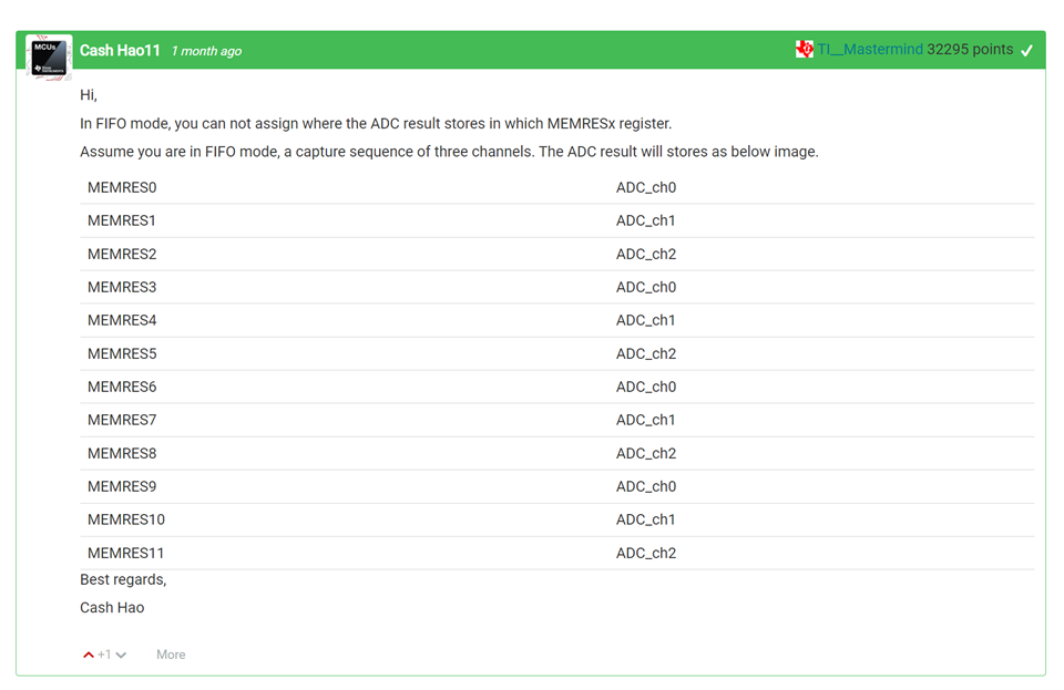
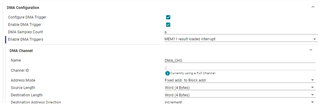
Hello, according to this table, when using the ADC with 4 channels, a DMA, and a FIFO, and toggling an LED each time the DL_ADC12_IIDX_DMA_DONE flag is set, does this mean that the flag will be set when the sampling value is loaded into MEMRES11 and not into MEMRES3?

  • Hi Ali,

    The DMA Done flag will trigger once the DMA has completed the number of transfers you set in the DMA configuration. If you have 4 transfers then DMA done will trigger after the 4th DMA transfer and is independent from loading.

    I recommend looking at the dma_ping_pong example for another dma adc example (this is located in the subsystems folder, same file level as examples)

    Regards,
    Luke

  • But here it states that the DMA starts transfering once the ADC fills all its memory register

    Best regards

    Ali

  • Hi Ali,

    In the DMA Ping Pong readme the highlighted statement is true because of the setting for the DMA triggers is set to the last register. 

    You can set the DMA to trigger before the last register, as the ADC and DMA will run simultaneously so you can time your ADC to finish before the DMA transfers MEM10 and MEM11. The DMA trigger value you can choose does depend on your sampling speed of the ADC.

    Alternatively (or additionally) you can set the Early Channel Interrupt bit for the DMA to trigger its DMA done before it has completely finished. This is helpful for an overall application speed because the DMA will eventually finish all of its transfers, but you can allow your CPU to handle the IRQ. See section 4.2.11 in the Technical Reference Manual.

    Regards,
    Luke

  • Hi Luke,

    my question is I have 4 ADC channels, and I have DMA and FIFO enabled. Can I configure the ADC so that the ADC triggers the DMA when the result is loaded to MEM3, or am I forced to wait because of the FIFO until MEM11 is loaded and then the ADC triggers the DMA to work? Because I noticed that if I toggle an LED every time DL_ADC12_IIDX_DMA_DONE is set, there is no difference whether the (Enable DMA Trigger) MEM5 resoult loaded interrupt, MEM11 resoult loaded interrupt or MEM3 resoult loaded interrupt, why?

    Regards,
    Ali

  • Hi Ali,

    Can you slow your sample rate down a lot and tell me if you still get the same result?

    Regards.
    Luke

  • Hi Luke,

    I slowed my sample rate from 10 µs to 31.25 ns, but I still get the same result.

    Best regards,

    Ali 

  • Hi Ali,

    I tested mine and at "Desired Sample time = 2ms" and I got 2.3416 ms per gpio toggle and at "Desired Sample time = 1ms" got 1.18ms per toggle. At faster ADC samples you might be getting the same result because the ADC to DMA is not your bottle neck in the process.

    Regards,
    Luke

  • Hi Luke,

    Do you use FIFO and DMA along with ADC? And does a timer triggers the ADC ? and how many channels are using in you example?

    Best Regads, 

    Ali 

  • Hi Luke,

    How would the code look like when using multiple channels in sequence with DMA and ADC but not using FIFO. Especially for the DL_DMA_setSrcAddr function. And what mode should I use for the DMA, Address Mode as well as Transfer Mode? 

    SYSCFG_DL_init();

    DL_DMA_setSrcAddr(DMA, DMA_CH0_CHAN_ID,
    (uint32_t) DL_ADC12_getMemResultAddress(ADC12_0_INST, DL_ADC12_MEM_IDX_0));

    DL_DMA_setDestAddr(DMA, DMA_CH0_CHAN_ID, (uint32_t) &gADCResult[0]);
    DL_DMA_setTransferSize(DMA, DMA_CH0_CHAN_ID, 2);

    DL_DMA_enableChannel(DMA, DMA_CH0_CHAN_ID);

    NVIC_EnableIRQ(ADC12_0_INST_INT_IRQN);

    Regards,
    Ali 

  • Hi Ali,

    I was using the FIFO and DMA. I took the DMA ping pong example code, switched to sequence and added a couple more channels, I also added a gpio to toggle from the DMA DONE interrupt.

    No timer was being used and repeat mode was on, so I didn't get the time difference between start to end of DMA done but between each DMA done transaction.

  • If not using the FIFO, I would line up the DMA to the number of channels you have. Remember the DMA will pull MEMRES at one time (if you have 4 channels then you will want 2 DMA transactions).

    The same settings that are used in the DMA ping pong or adc12_max_freq_dma can be used. The Address mode is fixed address to block address (ADC registers to your buffer/array). Transfer mode depends on your process flow with block transfer transferring the whole transfer size from a single trigger. Single trigger will require a trigger per transfer.

    I don't know your full application or how often this ADC process is taking place, but it sounds like you're periodically taking samples after every X amount of time. If you're planning on having all the data ready at once then using the block transfer to transfer all the data from the MEMRES registers to a buffer from a single DMA trigger.

    Regards
    Luke

  • Hi Luke, 

    If I want to use multiple ADC channels, how should the src function for the DMA look like?

    DL_DMA_setSrcAddr(DMA, DMA_CH0_CHAN_ID, (uint32_t) DL_ADC12_getMemResultAddress(ADC12_0_INST, DL_ADC12_MEM_IDX_0));
    

    I do not want to use FIFO and I want to use multiple channels. Is that possible?

    Regards 

    Ali

  • Hi Ali,

    You can use the DMA without FIFOs, the DMA setup would be the same except change the number of DMA samples to the number of channels you have divided by 2.

    Regards,
    Luke

  • Hi Luke,

    I tried to use only two channels without FIFO and it did not work. I was only getting the result from DL_ADC12_MEM_IDX_0, although I configured the DMA to increament source.

    This is my code:

    #include "ti_msp_dl_config.h"

    bool gCheckADC;
    uint16_t gADCResult[2];

    uint32_t addressone;
    uint32_t addresstwo;

    int main(void)
    {
    SYSCFG_DL_init();

    DL_DMA_setSrcAddr(DMA, DMA_CH0_CHAN_ID,
    (uint32_t) DL_ADC12_getMemResultAddress(ADC12_0_INST, DL_ADC12_MEM_IDX_0));

    DL_DMA_setDestAddr(DMA, DMA_CH0_CHAN_ID, (uint32_t) &gADCResult[0]);
    DL_DMA_setTransferSize(DMA, DMA_CH0_CHAN_ID, 2);

    DL_DMA_enableChannel(DMA, DMA_CH0_CHAN_ID);

    NVIC_EnableIRQ(ADC12_0_INST_INT_IRQN);

    DL_TimerG_startCounter(TIMER_0_INST);

    gCheckADC = false;

    while (gCheckADC == false)
    {
    __WFE();

    }


    __BKPT(0);

    addressone = DL_ADC12_getMemResultAddress(ADC12_0_INST, DL_ADC12_MEM_IDX_0);
    addresstwo = DL_ADC12_getMemResultAddress(ADC12_0_INST, DL_ADC12_MEM_IDX_1);

    while (1) {
    }
    }


    void ADC12_0_INST_IRQHandler(void)
    {
    switch (DL_ADC12_getPendingInterrupt(ADC12_0_INST)) {
    case DL_ADC12_IIDX_DMA_DONE:
    gCheckADC = true;
    //gADCResult[0] = DL_ADC12_getMemResult(ADC12_0_INST, DL_ADC12_MEM_IDX_0);
    // gADCResult[1] = DL_ADC12_getMemResult(ADC12_0_INST, DL_ADC12_MEM_IDX_1);
    // DL_ADC12_enableConversions(ADC12_0_INST);
    // DL_GPIO_togglePins(GPIO_LEDS_PORT, GPIO_LEDS_USER_LED_1_PIN);
    break;
    default:
    break;
    }
    }

    /*
    * ============ ti_msp_dl_config.c =============
    * Configured MSPM0 DriverLib module definitions
    *
    * DO NOT EDIT - This file is generated for the MSPM0G350X
    * by the SysConfig tool.
    */

    #include "ti_msp_dl_config.h"

    /*
    * ======== SYSCFG_DL_init ========
    * Perform any initialization needed before using any board APIs
    */
    SYSCONFIG_WEAK void SYSCFG_DL_init(void)
    {
    SYSCFG_DL_initPower();
    SYSCFG_DL_GPIO_init();
    /* Module-Specific Initializations*/
    SYSCFG_DL_SYSCTL_init();
    SYSCFG_DL_TIMER_0_init();
    SYSCFG_DL_ADC12_0_init();
    SYSCFG_DL_DMA_init();
    }

    SYSCONFIG_WEAK void SYSCFG_DL_initPower(void)
    {
    DL_GPIO_reset(GPIOA);
    DL_GPIO_reset(GPIOB);
    DL_TimerG_reset(TIMER_0_INST);
    DL_ADC12_reset(ADC12_0_INST);


    DL_GPIO_enablePower(GPIOA);
    DL_GPIO_enablePower(GPIOB);
    DL_TimerG_enablePower(TIMER_0_INST);
    DL_ADC12_enablePower(ADC12_0_INST);

    delay_cycles(POWER_STARTUP_DELAY);
    }

    SYSCONFIG_WEAK void SYSCFG_DL_GPIO_init(void)
    {

    DL_GPIO_initDigitalOutput(GPIO_LEDS_USER_LED_1_IOMUX);

    DL_GPIO_clearPins(GPIO_LEDS_PORT, GPIO_LEDS_USER_LED_1_PIN);
    DL_GPIO_enableOutput(GPIO_LEDS_PORT, GPIO_LEDS_USER_LED_1_PIN);

    }


    SYSCONFIG_WEAK void SYSCFG_DL_SYSCTL_init(void)
    {

    //Low Power Mode is configured to be SLEEP0
    DL_SYSCTL_setBORThreshold(DL_SYSCTL_BOR_THRESHOLD_LEVEL_0);

    DL_SYSCTL_setSYSOSCFreq(DL_SYSCTL_SYSOSC_FREQ_BASE);
    /* Set default configuration */
    DL_SYSCTL_disableHFXT();
    DL_SYSCTL_disableSYSPLL();
    DL_SYSCTL_setULPCLKDivider(DL_SYSCTL_ULPCLK_DIV_1);
    DL_SYSCTL_setMCLKDivider(DL_SYSCTL_MCLK_DIVIDER_DISABLE);

    }

    /*
    * Timer clock configuration to be sourced by BUSCLK / (32000000 Hz)
    * timerClkFreq = (timerClkSrc / (timerClkDivRatio * (timerClkPrescale + 1)))
    * 32000000 Hz = 32000000 Hz / (1 * (0 + 1))
    */
    static const DL_TimerG_ClockConfig gTIMER_0ClockConfig = {
    .clockSel = DL_TIMER_CLOCK_BUSCLK,
    .divideRatio = DL_TIMER_CLOCK_DIVIDE_1,
    .prescale = 0U,
    };

    /*
    * Timer load value (where the counter starts from) is calculated as (timerPeriod * timerClockFreq) - 1
    * TIMER_0_INST_LOAD_VALUE = (2 ms * 32000000 Hz) - 1
    */
    static const DL_TimerG_TimerConfig gTIMER_0TimerConfig = {
    .period = TIMER_0_INST_LOAD_VALUE,
    .timerMode = DL_TIMER_TIMER_MODE_PERIODIC,
    .startTimer = DL_TIMER_STOP,
    };

    SYSCONFIG_WEAK void SYSCFG_DL_TIMER_0_init(void) {

    DL_TimerG_setClockConfig(TIMER_0_INST,
    (DL_TimerG_ClockConfig *) &gTIMER_0ClockConfig);

    DL_TimerG_initTimerMode(TIMER_0_INST,
    (DL_TimerG_TimerConfig *) &gTIMER_0TimerConfig);
    DL_TimerG_enableClock(TIMER_0_INST);


    DL_TimerG_enableEvent(TIMER_0_INST, DL_TIMERG_EVENT_ROUTE_1, (DL_TIMERG_EVENT_ZERO_EVENT));

    DL_TimerG_setPublisherChanID(TIMER_0_INST, DL_TIMERG_PUBLISHER_INDEX_0, TIMER_0_INST_PUB_0_CH);

    }


    /* ADC12_0 Initialization */
    static const DL_ADC12_ClockConfig gADC12_0ClockConfig = {
    .clockSel = DL_ADC12_CLOCK_SYSOSC,
    .divideRatio = DL_ADC12_CLOCK_DIVIDE_1,
    .freqRange = DL_ADC12_CLOCK_FREQ_RANGE_24_TO_32,
    };
    SYSCONFIG_WEAK void SYSCFG_DL_ADC12_0_init(void)
    {
    DL_ADC12_setClockConfig(ADC12_0_INST, (DL_ADC12_ClockConfig *) &gADC12_0ClockConfig);

    DL_ADC12_initSeqSample(ADC12_0_INST,
    DL_ADC12_REPEAT_MODE_DISABLED, DL_ADC12_SAMPLING_SOURCE_AUTO, DL_ADC12_TRIG_SRC_EVENT,
    DL_ADC12_SEQ_START_ADDR_00, DL_ADC12_SEQ_END_ADDR_01, DL_ADC12_SAMP_CONV_RES_12_BIT,
    DL_ADC12_SAMP_CONV_DATA_FORMAT_UNSIGNED);
    DL_ADC12_configConversionMem(ADC12_0_INST, ADC12_0_ADCMEM_0,
    DL_ADC12_INPUT_CHAN_0, DL_ADC12_REFERENCE_VOLTAGE_VDDA, DL_ADC12_SAMPLE_TIMER_SOURCE_SCOMP0, DL_ADC12_AVERAGING_MODE_DISABLED,
    DL_ADC12_BURN_OUT_SOURCE_DISABLED, DL_ADC12_TRIGGER_MODE_AUTO_NEXT, DL_ADC12_WINDOWS_COMP_MODE_DISABLED);
    DL_ADC12_configConversionMem(ADC12_0_INST, ADC12_0_ADCMEM_1,
    DL_ADC12_INPUT_CHAN_1, DL_ADC12_REFERENCE_VOLTAGE_VDDA, DL_ADC12_SAMPLE_TIMER_SOURCE_SCOMP0, DL_ADC12_AVERAGING_MODE_DISABLED,
    DL_ADC12_BURN_OUT_SOURCE_DISABLED, DL_ADC12_TRIGGER_MODE_TRIGGER_NEXT, DL_ADC12_WINDOWS_COMP_MODE_DISABLED);
    DL_ADC12_enableFIFO(ADC12_0_INST);
    DL_ADC12_setPowerDownMode(ADC12_0_INST,DL_ADC12_POWER_DOWN_MODE_MANUAL);
    DL_ADC12_setSampleTime0(ADC12_0_INST,480);
    DL_ADC12_enableDMA(ADC12_0_INST);
    DL_ADC12_setDMASamplesCnt(ADC12_0_INST,2);
    DL_ADC12_enableDMATrigger(ADC12_0_INST,(DL_ADC12_DMA_MEM1_RESULT_LOADED));
    DL_ADC12_setSubscriberChanID(ADC12_0_INST,ADC12_0_INST_SUB_CH);
    /* Enable ADC12 interrupt */
    DL_ADC12_clearInterruptStatus(ADC12_0_INST,(DL_ADC12_INTERRUPT_MEM1_RESULT_LOADED));
    DL_ADC12_enableInterrupt(ADC12_0_INST,(DL_ADC12_INTERRUPT_MEM1_RESULT_LOADED));
    DL_ADC12_enableConversions(ADC12_0_INST);
    }

    static const DL_DMA_Config gDMA_CH0Config = {
    .transferMode = DL_DMA_SINGLE_BLOCK_TRANSFER_MODE,
    .extendedMode = DL_DMA_NORMAL_MODE,
    .destIncrement = DL_DMA_ADDR_INCREMENT,
    .srcIncrement = DL_DMA_ADDR_INCREMENT,
    .destWidth = DL_DMA_WIDTH_WORD,
    .srcWidth = DL_DMA_WIDTH_WORD,
    .trigger = ADC12_0_INST_DMA_TRIGGER,
    .triggerType = DL_DMA_TRIGGER_TYPE_EXTERNAL,
    };

    SYSCONFIG_WEAK void SYSCFG_DL_DMA_CH0_init(void)
    {
    DL_DMA_initChannel(DMA, DMA_CH0_CHAN_ID , (DL_DMA_Config *) &gDMA_CH0Config);
    }
    SYSCONFIG_WEAK void SYSCFG_DL_DMA_init(void){
    SYSCFG_DL_DMA_CH0_init();
    }

    Best Regards,

    Ali