This thread has been locked.

If you have a related question, please click the "Ask a related question" button in the top right corner. The newly created question will be automatically linked to this question.

MCU-PLUS-SDK-AM243X: AM2431 board custom flash programming problem.

Part Number: MCU-PLUS-SDK-AM243X
Other Parts Discussed in Thread: AM2431, UNIFLASH

Tool/software:

Dear TI experts,

I am working on AM2431 board with custom nor flash MT25QL256ABA. I have some problems during nor flash programming.

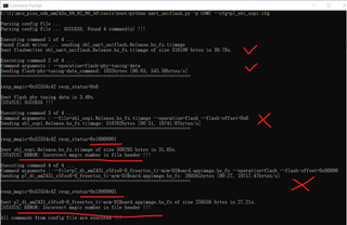
1. I set boot mode to Dev boot and use example project 'ospi_flash_diag_am243x-evm_r5fss0-0_nortos_ti-arm-clang' to get flash parameters.

Save flash parameters to json file  and load into project 'sbl_jtag_uniflash_am243x-evm_r5fss0-0_nortos_ti-arm-clang', 'sbl_uart_uniflash_am243x-evm_r5fss0-0_nortos_ti-arm-clang' and 'sbl_ospi_am243x-evm_r5fss0-0_nortos_ti-arm-clang' syscfg.

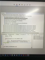
Then use jtag to debug project sbl_jtag_uniflash, erase, write, verify of flash are success.

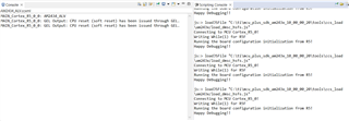
After that I change boot mode to QSPI mode, there is no log messages from uart terminal. It seems sbl_ospi doesn't work.

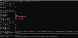
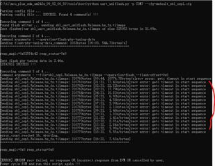
2. I set boot mode to UART, I use python script to download files. 2 of 4 files are transferred fail because of incorrect magic number.

Our DeviceType is HSFS.

I add some information in python script "print("resp_magic={} resp_status={}\n".format(hex(resp_magic), hex(resp_status)))".

I don't know how to continue. Need you help!

Best Regards,

  • Hello,

    The AM243x-EVM UART_UNIFLASH uses DDR for storing the received images over UART. In case you are using custom DDR, have you already integrated the corresponding DDR config file in the UNIFLASH examples?

    Regards,

    Prashant

  • We don't use custom DDR. But I don't know how to remove DDR from syscfg or other place. When i remove DDR from syscfg, flash-phy-tuning-data operation will fail.

  • If you don't have DDR on your custom board then you will have to modify the UART_UNIFLASH example to move the buffer from DDR to MSRAM. Please see the following link:

    e2e.ti.com/.../4788625

  • I changed linker.cmd and main,cpp as you said. But UART uniflash still fail:

  • Have the key programmed to board? I observed that the HS-FS image was programmed into flash memory and I think the key was not programmed. Please using the GP format image to try. 

  • I don't know how to generate GP format of sbl_ospi.release.tiimage. After I changed to SDK10.0 as you suggested, sbl_jtag_uniflash lp project can't import flash json file generated before.

    .

    Then I import SDK10.0 jtag_flash_diag project to read flash parameter, but it fails.

    The flash json file generated in SDK 9.02 is:

    {
    
    	"flashSize": 33554432,
    	"flashPageSize": 256,
    	"flashManfId": "0x20",
    	"flashDeviceId": "0xBA19",
    	"flashBlockSize": 65536,
    	"flashSectorSize": 4096,
    	"cmdBlockErase3B": "0xD8",
    	"cmdBlockErase4B": "0xDC",
    	"cmdSectorErase3B": "0x20",
    	"cmdSectorErase4B": "0x21",
    	"protos": {
    		"p111": {
    			"isDtr": false,
    			"cmdRd": "0x03",
    			"cmdWr": "0x02",
    			"modeClksCmd": 0,
    			"modeClksRd": 0,
    			"dummyClksCmd": 0,
    			"dummyClksRd": 0,
    			"enableType": "0",
    			"enableSeq": "0x00",
    			"dummyCfg": null,
    			"protoCfg": null,
    			"strDtrCfg": null
    		},
    		"p112": {
    			"isDtr": false,
    			"cmdRd": "0x3C",
    			"cmdWr": "0x02",
    			"modeClksCmd": 0,
    			"modeClksRd": 1,
    			"dummyClksCmd": 0,
    			"dummyClksRd": 7,
    			"enableType": "0",
    			"enableSeq": "0x00",
    			"dummyCfg": null,
    			"protoCfg": null,
    			"strDtrCfg": null
    		},
    		"p114": {
    			"isDtr": false,
    			"cmdRd": "0x6C",
    			"cmdWr": "0x34",
    			"modeClksCmd": 0,
    			"modeClksRd": 1,
    			"dummyClksCmd": 0,
    			"dummyClksRd": 7,
    			"enableType": "0",
    			"enableSeq": "0x00",
    			"dummyCfg": null,
    			"protoCfg": null,
    			"strDtrCfg": null
    		},
    		"p118": {
    			"isDtr": false,
    			"cmdRd": "0x7C",
    			"cmdWr": "0x84",
    			"modeClksCmd": 0,
    			"modeClksRd": 0,
    			"dummyClksCmd": 0,
    			"dummyClksRd": 0,
    			"enableType": "255",
    			"enableSeq": "0x00",
    			"dummyCfg": null,
    			"protoCfg": null,
    			"strDtrCfg": null
    		},
    		"p444s": {
    			"isDtr": false,
    			"cmdRd": "0xEB",
    			"cmdWr": "0x02",
    			"modeClksCmd": 0,
    			"modeClksRd": 1,
    			"dummyClksCmd": 0,
    			"dummyClksRd": 9,
    			"enableType": "0",
    			"enableSeq": "0x14",
    			"dummyCfg": {
    				"isAddrReg": false,
    				"cmdRegRd":"0x00",
    				"cmdRegWr":"0x00",
    				"cfgReg":"0x00000000",
    				"shift":0,
    				"mask":"0x00",
    				"bitP":0
    			},
    			"protoCfg": {
    				"isAddrReg": false,
    				"cmdRegRd": "0x00",
    				"cmdRegWr": "0x00",
    				"cfgReg": "0x00000000",
    				"shift": 0,
    				"mask": "0x00",
    				"bitP": 0
    			},
    			"strDtrCfg": {
    				"isAddrReg": false,
    				"cmdRegRd": "0x00",
    				"cmdRegWr": "0x00",
    				"cfgReg": "0x00000000",
    				"shift": 0,
    				"mask": "0x00",
    				"bitP": 0
    			}
    		},
    		"p444d": {
    			"isDtr": false,
    			"cmdRd": "0xEB",
    			"cmdWr": "0x02",
    			"modeClksCmd": 0,
    			"modeClksRd": 1,
    			"dummyClksCmd": 0,
    			"dummyClksRd": 9,
    			"enableType": "0",
    			"enableSeq": "0x14",
    			"dummyCfg": {
    				"isAddrReg": false,
    				"cmdRegRd":"0x00",
    				"cmdRegWr":"0x00",
    				"cfgReg":"0x00000000",
    				"shift":0,
    				"mask":"0x00",
    				"bitP":0
    			},
    			"protoCfg": {
    				"isAddrReg": false,
    				"cmdRegRd": "0x00",
    				"cmdRegWr": "0x00",
    				"cfgReg": "0x00000000",
    				"shift": 0,
    				"mask": "0x00",
    				"bitP": 0
    			},
    			"strDtrCfg": {
    				"isAddrReg": false,
    				"cmdRegRd": "0x00",
    				"cmdRegWr": "0x00",
    				"cfgReg": "0x00000000",
    				"shift": 0,
    				"mask": "0x00",
    				"bitP": 0
    			}
    		},
    		"p888s": null,
    		"p888d": null,
    		"pCustom": { 
    			"fxn": null
    		}
    	},
    	"addrByteSupport": "1",
    	"fourByteAddrEnSeq": "0x36",
    	"cmdExtType": "NONE",
    	"resetType": "0x3D",
    	"deviceBusyType": "0",
    	"cmdWren": "0x06",
    	"cmdRdsr": "0x05",
    	"srWip":  0,
    	"srWel":  0,
    	"cmdChipErase": "0xC7",
    	"rdIdSettings": {
    		"cmd": "0x9F",
    		"numBytes": 5,
    		"dummy4": 0,
    		"dummy8": 0
    	},
    	"xspiWipRdCmd": "0x00",
    	"xspiWipReg": "0x00000000",
    	"xspiWipBit": 0,
    	"flashDeviceBusyTimeout": 84000000,
    	"flashPageProgTimeout": 120
    }

    In Dev mode, each time run SDK10.0 java script command, there is no Soc initialization log message.

     '

  • Let me go through the information & get back to you.

    Thanks!

  • Hi LingYun,

       The flashDeviceId is 0xBA19, which means it works at 3.0 V. Could you please check the power supply and data signal waveform.  The note here is the default EVM board Nor Flash power supply is 1.8V. Your design should be different to us. 

    Linjun

  • Hi Linjun,

    Today we use ospi_flash_io_am243x-evm project to write&read flash successfully. Flash protocol is 1s-1s-1s. The key point is that

    Each time we change syscfg 'Protocol', we need to LOAD FROM JSON again. The CCS tool will fill flash parameters with json file according to current 'Protocol' value.

    And we also test Protocol 1s-1s-4s, but it failed. The problem occurs on reading data:

    I will ask for MICRON for this problem. Do you have any idea and be free to tell me.

  • Hi Lingyun,

       Please upload the schematics and PCB layout there, the OSPI power supply need our hardware expert to review.  Thanks.

    Linjun

  • When I changed FLASH protocol 1s-1s-4s, dummy clock read = 0(json value is 7), OSPI clock input=200M, divider=4, the flash read&write are both Ok.

    So I did some tests:

    1. Use JTAG uniflash to write sbl-null into flash. When switch boot mode to QSPI, sbl-null works.

    2. Use UART uniflash to write sbl-null into flash, When switch boot mode to QSPI, sbl-null works.

    3. Recompile sbl-ospi with the above FLASH parameters. Use UART uniflash to write sbl-ospi and hello world. When switch boot mode to QSPI, sbl-ospi print some info and hello world print nothing.

    So I add loop_forever in sbl-ospi main(), connect with JTAG and debug.

    From the callstack, we can see the sbl-ospi is blocked in Bootloader_parseMultiCoreAppImage->Bootloader_verifyMulticoreImage->Bootloader_getMsgLen->Bootloader_findSeq. Once accessing x509_cert_ptr(0x6008000), it crash.

  • Lingyun,

      Could you please upload the project  example.syscfg here to check the what's the bootloader setting? Thanks.

    Linjun

  • Please find the attachment for example.syscfg and sbl_ospi.Debug.map.

    /**
     * These arguments were used when this file was generated. They will be automatically applied on subsequent loads
     * via the GUI or CLI. Run CLI with '--help' for additional information on how to override these arguments.
     * @cliArgs --device "AM243x_ALV_beta" --package "ALV" --part "ALV" --context "r5fss0-0" --product "MCU_PLUS_SDK_AM243x@09.02.00"
     * @versions {"tool":"1.20.0+3587"}
     */
    
    /**
     * Import the modules used in this configuration.
     */
    const flash           = scripting.addModule("/board/flash/flash", {}, false);
    const flash1          = flash.addInstance();
    const bootloader      = scripting.addModule("/drivers/bootloader/bootloader", {}, false);
    const bootloader1     = bootloader.addInstance();
    const ddr             = scripting.addModule("/drivers/ddr/ddr", {}, false);
    const ddr1            = ddr.addInstance();
    const debug_log       = scripting.addModule("/kernel/dpl/debug_log");
    const mpu_armv7       = scripting.addModule("/kernel/dpl/mpu_armv7", {}, false);
    const mpu_armv71      = mpu_armv7.addInstance();
    const mpu_armv72      = mpu_armv7.addInstance();
    const mpu_armv73      = mpu_armv7.addInstance();
    const mpu_armv74      = mpu_armv7.addInstance();
    const mpu_armv75      = mpu_armv7.addInstance();
    const default_linker  = scripting.addModule("/memory_configurator/default_linker", {}, false);
    const default_linker1 = default_linker.addInstance();
    const general         = scripting.addModule("/memory_configurator/general", {}, false);
    const general1        = general.addInstance();
    const region          = scripting.addModule("/memory_configurator/region", {}, false);
    const region1         = region.addInstance();
    const section         = scripting.addModule("/memory_configurator/section", {}, false);
    const section1        = section.addInstance();
    const section2        = section.addInstance();
    const section3        = section.addInstance();
    const section4        = section.addInstance();
    
    /**
     * Write custom configuration values to the imported modules.
     */
    bootloader1.appImageOffset      = "0x80000";
    bootloader1.$name               = "CONFIG_BOOTLOADER_FLASH0";
    bootloader1.appImageBaseAddress = "0x60080000";
    bootloader1.disableAppImageAuth = true;
    
    flash1.$name                           = "CONFIG_FLASH0";
    bootloader1.flashDriver                = flash1;
    flash1.device                          = "CUSTOM_FLASH";
    flash1.fname                           = "P7";
    flash1.flashSize                       = 33554432;
    flash1.flashManfId                     = "0x20";
    flash1.flashDeviceId                   = "0xBA19";
    flash1.flashBlockSize                  = 65536;
    flash1.cmdBlockErase3B                 = "0xD8";
    flash1.cmdSectorErase3B                = "0x20";
    flash1.dummyClksCmd                    = 0;
    flash1.proto_isAddrReg                 = false;
    flash1.dummy_isAddrReg                 = false;
    flash1.strDtr_isAddrReg                = false;
    flash1.resetType                       = "0x3D";
    flash1.deviceBusyType                  = "0";
    flash1.cmdExtType                      = "NONE";
    flash1.srWel                           = 0;
    flash1.xspiWipRdCmd                    = "0x00";
    flash1.xspiWipReg                      = "0x00000000";
    flash1.idNumBytes                      = 5;
    flash1.dummyId8                        = 0;
    flash1.fourByteEnableSeq               = "0x36";
    flash1.flashDeviceBusyTimeout          = 84000000;
    flash1.flashPageProgTimeout            = 120;
    flash1.protocol                        = "1s_1s_4s";
    flash1.cmdRd                           = "0x6C";
    flash1.cmdWr                           = "0x34";
    flash1.modeClksRd                      = 1;
    flash1.dummyClksRd                     = 0;
    flash1.peripheralDriver.$name          = "CONFIG_OSPI0";
    flash1.peripheralDriver.advanced       = true;
    flash1.peripheralDriver.frmFmt         = "POL1_PHA1";
    flash1.peripheralDriver.inputClkFreq   = 200000000;
    flash1.peripheralDriver.OSPI.DQS.$used = false;
    flash1.peripheralDriver.OSPI.D7.rx     = false;
    flash1.peripheralDriver.OSPI.D7.$used  = false;
    flash1.peripheralDriver.OSPI.D6.rx     = false;
    flash1.peripheralDriver.OSPI.D6.$used  = false;
    flash1.peripheralDriver.OSPI.D5.rx     = false;
    flash1.peripheralDriver.OSPI.D5.$used  = false;
    flash1.peripheralDriver.OSPI.D4.rx     = false;
    flash1.peripheralDriver.OSPI.D4.$used  = false;
    
    ddr1.$name = "CONFIG_DDR0";
    
    debug_log.enableUartLog        = true;
    debug_log.enableLogZoneInfo    = true;
    debug_log.enableMemLog         = true;
    debug_log.uartLog.$name        = "CONFIG_UART0";
    debug_log.uartLog.intrEnable   = "DISABLE";
    debug_log.uartLog.UART.$assign = "USART0";
    
    const uart_v0_template  = scripting.addModule("/drivers/uart/v0/uart_v0_template", {}, false);
    const uart_v0_template1 = uart_v0_template.addInstance({}, false);
    uart_v0_template1.$name = "drivers_uart_v0_uart_v0_template0";
    debug_log.uartLog.child = uart_v0_template1;
    
    mpu_armv71.$name             = "CONFIG_MPU_REGION0";
    mpu_armv71.size              = 31;
    mpu_armv71.attributes        = "Device";
    mpu_armv71.accessPermissions = "Supervisor RD+WR, User RD";
    mpu_armv71.allowExecute      = false;
    
    mpu_armv72.$name             = "CONFIG_MPU_REGION1";
    mpu_armv72.size              = 15;
    mpu_armv72.accessPermissions = "Supervisor RD+WR, User RD";
    
    mpu_armv73.$name             = "CONFIG_MPU_REGION2";
    mpu_armv73.baseAddr          = 0x41010000;
    mpu_armv73.size              = 15;
    mpu_armv73.accessPermissions = "Supervisor RD+WR, User RD";
    
    mpu_armv74.$name             = "CONFIG_MPU_REGION3";
    mpu_armv74.accessPermissions = "Supervisor RD+WR, User RD";
    mpu_armv74.baseAddr          = 0x70000000;
    mpu_armv74.size              = 21;
    
    mpu_armv75.$name    = "CONFIG_MPU_REGION4";
    mpu_armv75.baseAddr = 0x80000000;
    mpu_armv75.size     = 31;
    
    default_linker1.$name = "memory_configurator_default_linker0";
    
    general1.$name          = "CONFIG_GENERAL0";
    general1.irq_stack_size = 4096;
    general1.svc_stack_size = 256;
    general1.entry_point    = "-e_vectors_sbl";
    general1.linker.$name   = "TIARMCLANG0";
    
    region1.$name                               = "MEMORY_REGION_CONFIGURATION0";
    region1.memory_region.create(6);
    region1.memory_region[0].type               = "TCMA_R5F";
    region1.memory_region[0].$name              = "R5F_VECS";
    region1.memory_region[0].size               = 0x40;
    region1.memory_region[0].auto               = false;
    region1.memory_region[1].type               = "TCMA_R5F";
    region1.memory_region[1].$name              = "R5F_TCMA";
    region1.memory_region[1].size               = 0x7FC0;
    region1.memory_region[2].type               = "TCMB_R5F";
    region1.memory_region[2].$name              = "R5F_TCMB0";
    region1.memory_region[2].size               = 0x8000;
    region1.memory_region[3].$name              = "MSRAM_VECS";
    region1.memory_region[3].auto               = false;
    region1.memory_region[3].size               = 0x100;
    region1.memory_region[4].$name              = "MSRAM_0";
    region1.memory_region[4].auto               = false;
    region1.memory_region[4].manualStartAddress = 0x70000100;
    region1.memory_region[4].size               = 0x6FF00;
    region1.memory_region[5].$name              = "MSRAM_1";
    region1.memory_region[5].auto               = false;
    region1.memory_region[5].manualStartAddress = 0x70070000;
    region1.memory_region[5].size               = 0x10000;
    
    section1.$name                        = "Vector Table";
    section1.group                        = false;
    section1.load_memory                  = "MSRAM_VECS";
    section1.output_section.create(1);
    section1.output_section[0].$name      = ".vectors";
    section1.output_section[0].palignment = true;
    
    section2.$name                        = "Text Segments";
    section2.load_memory                  = "MSRAM_0";
    section2.output_section.create(7);
    section2.output_section[0].palignment = true;
    section2.output_section[0].$name      = ".text";
    section2.output_section[1].palignment = true;
    section2.output_section[1].$name      = ".text.hwi";
    section2.output_section[2].palignment = true;
    section2.output_section[2].$name      = ".text.cache";
    section2.output_section[3].palignment = true;
    section2.output_section[3].$name      = ".text.mpu";
    section2.output_section[4].palignment = true;
    section2.output_section[4].$name      = ".text.boot";
    section2.output_section[5].$name      = ".data";
    section2.output_section[5].palignment = true;
    section2.output_section[6].$name      = ".rodata";
    section2.output_section[6].palignment = true;
    
    section3.$name                                   = "Memory Segments";
    section3.group                                   = false;
    section3.load_memory                             = "MSRAM_1";
    section3.output_section.create(3);
    section3.output_section[0].$name                 = ".bss";
    section3.output_section[0].palignment            = true;
    section3.output_section[0].output_sections_start = "__BSS_START";
    section3.output_section[0].output_sections_end   = "__BSS_END";
    section3.output_section[1].$name                 = ".sysmem";
    section3.output_section[1].palignment            = true;
    section3.output_section[2].$name                 = ".stack";
    section3.output_section[2].palignment            = true;
    
    section4.$name                                    = "Stack Segments";
    section4.load_memory                              = "MSRAM_1";
    section4.output_section.create(5);
    section4.output_section[0].$name                  = ".irqstack";
    section4.output_section[0].output_sections_start  = "__IRQ_STACK_START";
    section4.output_section[0].output_sections_end    = "__IRQ_STACK_END";
    section4.output_section[0].input_section.create(1);
    section4.output_section[0].input_section[0].$name = ". = . + __IRQ_STACK_SIZE;";
    section4.output_section[1].$name                  = ".fiqstack";
    section4.output_section[1].output_sections_start  = "__FIQ_STACK_START";
    section4.output_section[1].output_sections_end    = "__FIQ_STACK_END";
    section4.output_section[1].input_section.create(1);
    section4.output_section[1].input_section[0].$name = ". = . + __FIQ_STACK_SIZE;";
    section4.output_section[2].$name                  = ".svcstack";
    section4.output_section[2].output_sections_start  = "__SVC_STACK_START";
    section4.output_section[2].output_sections_end    = "__SVC_STACK_END";
    section4.output_section[2].input_section.create(1);
    section4.output_section[2].input_section[0].$name = ". = . + __SVC_STACK_SIZE;";
    section4.output_section[3].$name                  = ".abortstack";
    section4.output_section[3].output_sections_start  = "__ABORT_STACK_START";
    section4.output_section[3].output_sections_end    = "__ABORT_STACK_END";
    section4.output_section[3].input_section.create(1);
    section4.output_section[3].input_section[0].$name = ". = . + __ABORT_STACK_SIZE;";
    section4.output_section[4].$name                  = ".undefinedstack";
    section4.output_section[4].output_sections_start  = "__UNDEFINED_STACK_START";
    section4.output_section[4].output_sections_end    = "__UNDEFINED_STACK_END";
    section4.output_section[4].input_section.create(1);
    section4.output_section[4].input_section[0].$name = ". = . + __UNDEFINED_STACK_SIZE;";
    
    /**
     * Pinmux solution for unlocked pins/peripherals. This ensures that minor changes to the automatic solver in a future
     * version of the tool will not impact the pinmux you originally saw.  These lines can be completely deleted in order to
     * re-solve from scratch.
     */
    flash1.peripheralDriver.OSPI.$suggestSolution      = "OSPI0";
    flash1.peripheralDriver.OSPI.CLK.$suggestSolution  = "OSPI0_CLK";
    flash1.peripheralDriver.OSPI.CSn0.$suggestSolution = "OSPI0_CSn0";
    flash1.peripheralDriver.OSPI.D3.$suggestSolution   = "OSPI0_D3";
    flash1.peripheralDriver.OSPI.D2.$suggestSolution   = "OSPI0_D2";
    flash1.peripheralDriver.OSPI.D1.$suggestSolution   = "OSPI0_D1";
    flash1.peripheralDriver.OSPI.D0.$suggestSolution   = "OSPI0_D0";
    debug_log.uartLog.UART.RXD.$suggestSolution        = "UART0_RXD";
    debug_log.uartLog.UART.TXD.$suggestSolution        = "UART0_TXD";
    
    sbl_ospi.Debug.map.txt